While magnetron sputtering is a dominant industrial process for thin film deposition, its primary limitations are high initial equipment costs, inefficient use of the source material, challenges in depositing insulating materials at high rates, and the potential for unwanted heating of the substrate.
Magnetron sputtering is a remarkably versatile and powerful coating technology. However, its core limitations are not flaws but direct consequences of its underlying physics—the use of a magnetically-confined plasma to bombard a target—which creates specific trade-offs in cost, material efficiency, and process compatibility.
The Source of Limitations: Process Physics
Magnetron sputtering's greatest strengths—dense films, strong adhesion, and material flexibility—are derived from its energetic nature. Understanding that the limitations also stem from this same energetic process is key to making an informed decision.
Inefficient Target Material Utilization
The magnetic field used to trap electrons and enhance the plasma creates a concentrated erosion zone on the target's surface, often called a "racetrack."
This means only a fraction of the expensive target material, typically just 20-40%, is actually consumed before the target must be replaced. This drives up the operational cost, especially when using precious materials.
The Dielectric Deposition Hurdle
Sputtering works by bombarding a target with positive ions (like Argon, Ar+). When sputtering a conductive metal target, the positive charge is neutralized by the power supply.
However, with a dielectric (insulating) material, this positive charge builds up on the target's surface. This phenomenon, known as "target poisoning," repels the incoming positive ions and effectively shuts down the sputtering process.
The solution is to use a Radio Frequency (RF) power supply, but this introduces its own compromises: significantly lower deposition rates and more complex, expensive equipment.
Unwanted Substrate Heating
The deposition process is not gentle. The substrate is bombarded by high-energy sputtered atoms and reflected neutral atoms from the target.
This energy transfer results in significant substrate heating. This can be detrimental to temperature-sensitive materials like polymers, organic electronics, or biological samples, potentially causing damage or deformation.
Low Directionality and Shadowing
Unlike evaporative techniques where material travels in a line-of-sight path, sputtered atoms are ejected from the target over a very wide range of angles.
This lack of directionality makes it difficult to uniformly coat complex, three-dimensional surfaces with high-aspect-ratio features. It can lead to poor "step coverage" or shadowing effects, where some areas of the substrate receive little to no coating.
Understanding the Economic and Operational Trade-offs
Beyond the physics, the practical implementation of magnetron sputtering presents significant economic and operational considerations that must be factored into any project.
High Initial System Cost
A complete magnetron sputtering system is a complex piece of capital equipment.
The cost is driven by the need for a high-vacuum chamber, powerful and precise power supplies (DC or RF), magnetic assemblies, process gas handling systems, and sophisticated control software. This initial investment is often much higher than for simpler methods like thermal evaporation.
Process Complexity and Control
Achieving a stable, repeatable sputtering process requires a skilled operator. The quality of the final film depends on a sensitive balance of multiple variables, including gas pressure, power, temperature, and system geometry.
The plasma itself can exhibit instabilities, which can affect film uniformity and quality. This complexity means that process development can be both time-consuming and resource-intensive.
Making the Right Choice for Your Application
Ultimately, the decision to use magnetron sputtering depends on whether its advantages in film quality outweigh its inherent limitations for your specific goal.
- If your primary focus is high-volume deposition of metals or conductive films: Sputtering is an excellent choice for its speed and quality, but be sure to budget for the recurring cost of replacing inefficiently used targets.
- If your primary focus is depositing high-quality insulating films: Be prepared for the slower deposition rates and higher equipment complexity associated with the necessary RF sputtering process.
- If you are working with heat-sensitive substrates: You must determine if substrate cooling is feasible or if a less energetic deposition method is a more appropriate choice.
- If you require uniform coating on complex 3D shapes: You may need to incorporate substrate rotation or consider alternative technologies like Atomic Layer Deposition (ALD) to avoid shadowing effects.
By carefully weighing these limitations against its powerful benefits, you can determine if magnetron sputtering is the optimal path for achieving your material deposition goals.
Summary Table:
| Limitation | Key Impact |
|---|---|
| High Initial Cost | Significant capital investment for vacuum systems and power supplies. |
| Inefficient Material Use | Only 20-40% of the target material is typically consumed. |
| Challenges with Insulators | Requires complex RF sputtering, leading to lower deposition rates. |
| Substrate Heating | Can damage temperature-sensitive materials like polymers. |
| Low Directionality | Poor step coverage on complex 3D surfaces due to shadowing. |
Need help selecting the right thin film deposition technology for your lab?
The limitations of magnetron sputtering highlight the importance of matching your process to your specific application. At KINTEK, we specialize in lab equipment and consumables, offering expert guidance to help you navigate these trade-offs. Whether you're working with conductive metals, delicate insulating materials, or temperature-sensitive substrates, we can help you find the most efficient and cost-effective solution.
Contact us today via our [#ContactForm] to discuss your project requirements and discover how our expertise can enhance your laboratory's capabilities and outcomes.
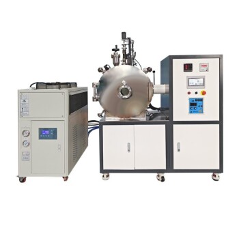
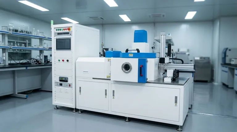
Visual Guide

Related Products
- Microwave Plasma Chemical Vapor Deposition MPCVD Machine System Reactor for Lab and Diamond Growth
- Chemical Vapor Deposition CVD Equipment System Chamber Slide PECVD Tube Furnace with Liquid Gasifier PECVD Machine
- Molybdenum Tungsten Tantalum Special Shape Evaporation Boat
- Hemispherical Bottom Tungsten Molybdenum Evaporation Boat
- Inclined Rotary Plasma Enhanced Chemical Vapor Deposition PECVD Equipment Tube Furnace Machine
People Also Ask
- How do vacuum pumps and valves collaborate in MPCVD? Achieve Precise Pressure Control for Superior CNT Synthesis
- How does a microwave plasma reactor facilitate the synthesis of diamond? Master MPCVD with Precision Technology
- What is microwave plasma chemical vapor deposition? A Guide to High-Purity Diamond Film Growth
- What are the primary advantages of the CVD method for growing diamonds? Engineering High-Purity Gems and Components
- Why is argon-rich gas phase chemistry used for UNCD growth? Unlock Precision Nano-Diamond Synthesis