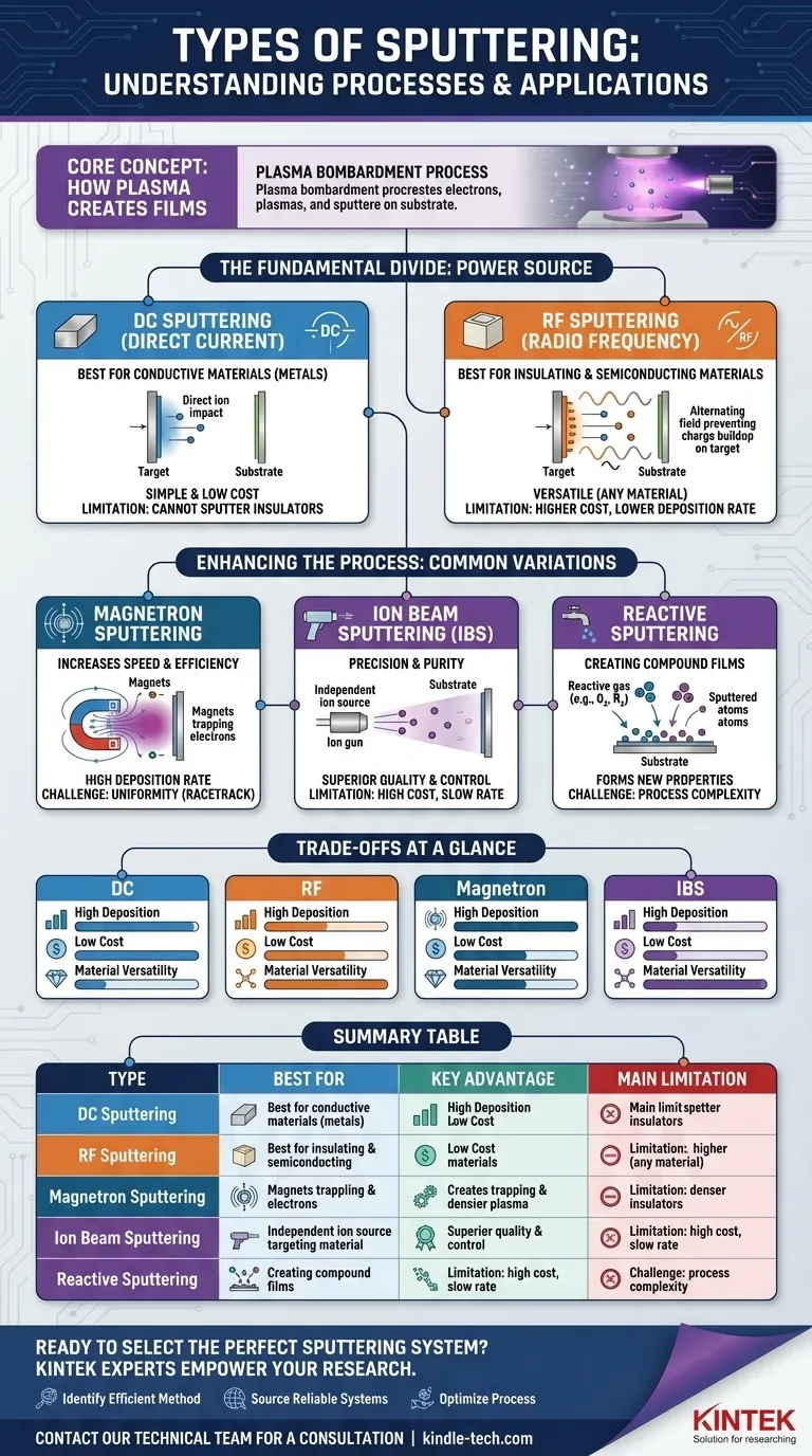
At its core, sputtering is categorized by how energy is supplied to create a plasma and bombard a target material. The most fundamental types are DC (Direct Current) sputtering, which is highly effective for electrically conductive materials, and RF (Radio Frequency) sputtering, which uses an alternating field to deposit non-conductive, insulating materials. Other important variations, such as Magnetron, Ion Beam, and Reactive sputtering, are enhancements designed to improve deposition speed, film quality, or create new compound materials.
The type of sputtering you choose is not a matter of preference but a direct consequence of your material. The fundamental choice between DC and RF is determined by whether your target material conducts electricity, while other methods are chosen to enhance deposition rate, film purity, or chemical composition.
The Fundamental Divide: Power Source
The primary distinction between sputtering methods comes down to the type of power supply used. This choice is dictated by the electrical conductivity of the material you intend to deposit.
DC Sputtering: The Workhorse for Metals
DC (Direct Current) sputtering is the simplest form of the technique. A high DC voltage is applied to the target material (the cathode) inside a low-pressure vacuum chamber, typically filled with an inert gas like Argon.
This high voltage ignites a plasma. Positively charged Argon ions are accelerated toward the negatively charged target, striking it with enough force to dislodge or "sputter" atoms. These sputtered atoms then travel and deposit onto the substrate, forming a thin film.
The critical limitation of DC sputtering is that it only works with conductive target materials.
RF Sputtering: The Solution for Insulators
If you try to use DC sputtering on an insulating target (like a ceramic), positive ions will quickly accumulate on its surface. This buildup of positive charge, known as "target poisoning," effectively neutralizes the negative voltage and shuts down the sputtering process.
RF (Radio Frequency) sputtering solves this by using a high-frequency alternating power source instead of a DC one. The field rapidly alternates between positive and negative, attracting electrons and then ions in alternating cycles.
This alternating bombardment prevents charge from building up, allowing for the effective sputtering of insulating and semiconducting materials. RF systems can also operate at lower gas pressures, which can improve film quality.
Enhancing the Process: Common Sputtering Variations
Beyond the basic power source, several key methodologies have been developed to optimize the sputtering process for speed, control, and film composition.
Magnetron Sputtering: Increasing Speed and Efficiency
Magnetron sputtering is an enhancement that can be applied to both DC and RF systems. It involves placing strong magnets behind the target.
These magnets trap electrons in a magnetic field directly in front of the target. This dramatically increases the probability that an electron will collide with an Argon atom, creating a much denser plasma for the same power input.
The result is a significantly higher deposition rate and less substrate heating, making Magnetron sputtering the dominant method for most industrial applications.
Ion Beam Sputtering (IBS): Precision and Purity
In Ion Beam Sputtering, the plasma generation is physically separated from the target. An independent ion source, or "gun," generates a focused beam of ions that is then aimed at the sputtering target.
This separation gives you independent control over ion energy and ion current. IBS allows for the creation of exceptionally high-quality, dense, and pure films with precise thickness control, making it ideal for high-performance optical coatings and advanced electronics.
Reactive Sputtering: Creating Compound Films
Reactive sputtering is a process, not a distinct hardware type. It involves intentionally introducing a reactive gas (like oxygen or nitrogen) into the vacuum chamber along with the inert sputtering gas (Argon).
As atoms are sputtered from a metallic target (e.g., Titanium), they react with this gas either in transit or on the substrate surface. This allows you to form compound films like Titanium Nitride (TiN) or Silicon Dioxide (SiO₂), which have drastically different properties than the original target material.
Understanding the Trade-offs
Each sputtering method offers a unique balance of capabilities, complexity, and cost. Understanding these trade-offs is key to selecting the right process.
DC Sputtering: Simplicity vs. Limitation
The primary advantage of DC sputtering is its simplicity and lower equipment cost. However, it is strictly limited to depositing electrically conductive materials, which is a significant constraint.
RF Sputtering: Versatility vs. Complexity
RF sputtering's main benefit is its ability to deposit literally any material, conductive or insulating. The trade-off is higher complexity and cost for the RF power supply and impedance matching network, as well as generally lower deposition rates compared to DC magnetron.
Magnetron Sputtering: Speed vs. Uniformity Challenges
The clear advantage of magnetron sputtering is its high deposition rate, which is crucial for manufacturing. A potential pitfall is that the magnetic field creates a non-uniform erosion pattern on the target (a "racetrack"), which can affect film uniformity and target material utilization if not properly managed.
Ion Beam Sputtering: Quality vs. Cost and Speed
IBS produces films with unparalleled quality, density, and purity. This performance comes at the cost of much slower deposition rates and significantly higher equipment cost and complexity compared to magnetron-based systems.
Making the Right Choice for Your Application
Your choice of sputtering technique should be driven by a clear understanding of your material requirements and project goals.
- If your primary focus is depositing conductive films (like metals) quickly and cost-effectively: DC Magnetron Sputtering is the industry standard and most efficient choice.
- If your primary focus is depositing insulating films (like oxides or ceramics): RF Sputtering is your necessary choice, and it is almost always paired with a magnetron to achieve practical deposition rates.
- If your primary focus is creating a specific compound film (like titanium nitride): Reactive Sputtering is the correct process, typically using a DC or RF magnetron system.
- If your primary focus is achieving the highest possible film purity and density for demanding optics or electronics: Ion Beam Sputtering (IBS) provides superior control and film quality, justifying its higher cost and complexity.
Understanding these core distinctions empowers you to select the precise sputtering technique that aligns with your material, budget, and desired film quality.
Summary Table:
| Sputtering Type | Best For | Key Advantage | Main Limitation |
|---|---|---|---|
| DC Sputtering | Conductive Materials (Metals) | Simple, Low Cost | Cannot Sputter Insulators |
| RF Sputtering | Insulating & Semiconducting Materials | Versatile (Any Material) | Higher Cost, Lower Deposition Rate |
| Magnetron Sputtering | High-Speed Deposition (Industrial) | High Deposition Rate, Efficient | Potential Uniformity Challenges |
| Ion Beam Sputtering (IBS) | High-Purity Films (Optics, Electronics) | Superior Film Quality & Control | High Cost, Slow Deposition |
| Reactive Sputtering | Creating Compound Films (e.g., TiN, SiO₂) | Forms New Material Properties | Process Complexity |
Ready to Select the Perfect Sputtering System for Your Lab?
Choosing the right sputtering technique is critical for achieving your desired thin-film properties, whether you're working with metals, ceramics, or complex compounds. The experts at KINTEK specialize in providing the ideal lab equipment solutions for your specific deposition challenges.
We can help you:
- Identify the most efficient and cost-effective method for your materials and application.
- Source reliable DC, RF, Magnetron, or Ion Beam Sputtering systems that deliver consistent, high-quality results.
- Optimize your process for better film uniformity, purity, and deposition rates.
Don't leave your project's success to chance. Contact our technical team today for a personalized consultation and let KINTEK empower your research and development with precision sputtering solutions.
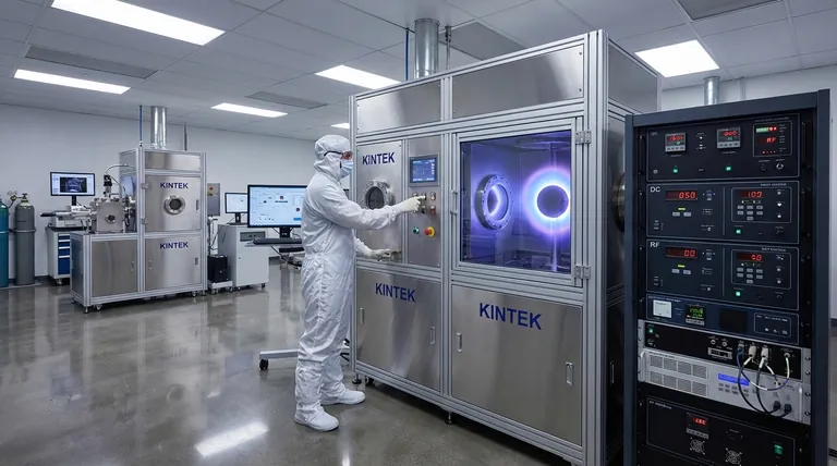
Visual Guide
Related Products
- Spark Plasma Sintering Furnace SPS Furnace
- Vacuum Induction Melting Spinning System Arc Melting Furnace
- Chemical Vapor Deposition CVD Equipment System Chamber Slide PECVD Tube Furnace with Liquid Gasifier PECVD Machine
People Also Ask
- Why are Spark Plasma Sintering (SPS) furnaces or hot presses utilized in the preparation of Li3PS4 solid electrolytes?
- What is the difference between spark plasma sintering and flash sintering? A Guide to Advanced Sintering Methods
- What is the mechanism of SPS process? A Deep Dive into Rapid, Low-Temperature Sintering
- What is SPS sintering method? A Guide to High-Speed, High-Performance Material Fabrication
- What are the fundamentals of spark plasma sintering process? Unlock Rapid, High-Performance Material Consolidation


