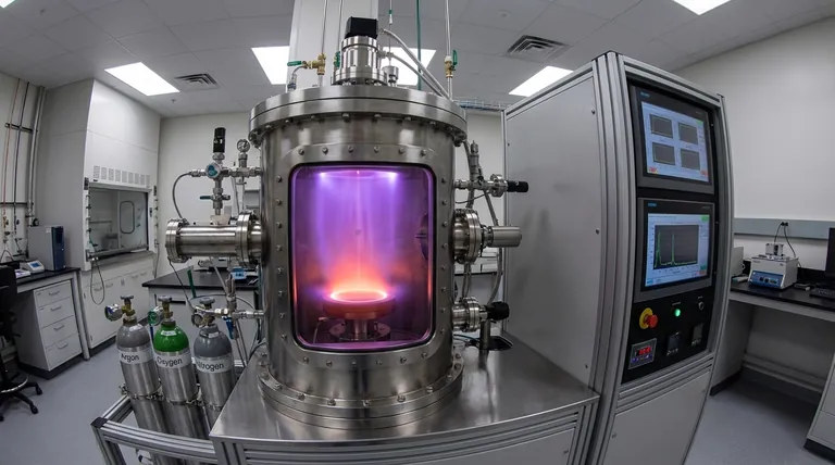
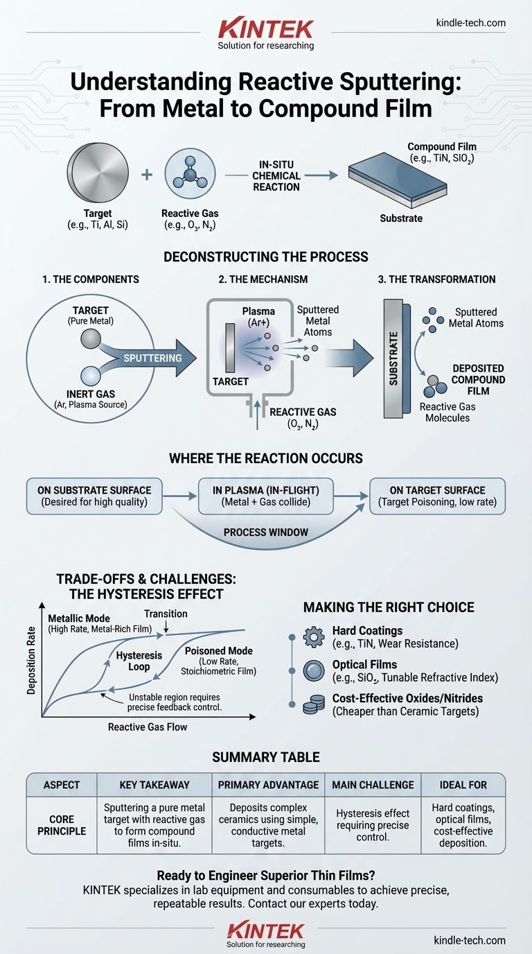
In essence, reactive sputtering is a physical vapor deposition (PVD) technique for creating high-quality compound thin films. It enhances the standard sputtering process by introducing a chemically reactive gas, such as oxygen or nitrogen, into the vacuum chamber alongside the typical inert gas. This reactive gas combines with the atoms sputtered from a pure target material, forming a new compound—like an oxide or nitride—that deposits onto the substrate.
The core challenge in thin film deposition is creating complex compound materials, like ceramics, which are often difficult to sputter directly. Reactive sputtering elegantly solves this by starting with a simple, easy-to-sputter metallic target and forming the desired compound in-situ by adding a controlled amount of reactive gas to the process.
Deconstructing the Reactive Sputtering Process
To grasp reactive sputtering, it's best to understand its fundamental components and how they interact. The process is a careful balance of physical bombardment and chemical reaction.
The Core Components
- The Target: This is the source material, typically a high-purity metal like titanium (Ti), aluminum (Al), or silicon (Si). This target is what gets sputtered.
- The Inert Gas: Almost always Argon (Ar). Argon atoms are ionized to create a plasma. These heavy ions are accelerated into the target, acting like atomic-scale sandblasters that physically knock target atoms loose.
- The Reactive Gas: This is the "special ingredient," such as Oxygen (O₂), Nitrogen (N₂), or a hydrocarbon like Acetylene (C₂H₂). This gas is what enables the chemical transformation.
The Sputtering Mechanism
The process begins like any standard sputtering deposition. A high voltage is applied in the low-pressure argon environment, creating a plasma of argon ions and electrons. The positively charged argon ions are drawn forcefully toward the negatively charged target, striking its surface and ejecting (sputtering) neutral target atoms.
The "Reactive" Transformation
The key difference happens next. As the sputtered metal atoms travel toward the substrate, they encounter the reactive gas that has been intentionally bled into the chamber. This triggers a chemical reaction, forming a new compound molecule that then deposits onto the substrate as a thin film.
Where Does the Chemical Reaction Occur?
The location of the chemical reaction is not a single point, but a dynamic process that can happen in several places. Controlling which one dominates is key to mastering the technique.
On the Substrate Surface
This is often the most desired mechanism for high-quality films. Individual metal atoms from the target and molecules of the reactive gas arrive at the substrate surface separately, where they combine to grow the compound film layer by layer.
In the Plasma (In-Flight)
Sputtered metal atoms can collide and react with the reactive gas molecules mid-flight, between the target and the substrate. These newly formed compound molecules then continue their journey to the substrate.
On the Target Surface
If the reactive gas pressure is too high, the gas can begin to react directly with the surface of the target itself. This is known as "target poisoning." A thin layer of the compound (e.g., an oxide or nitride) forms on the target, which has significant consequences for the process.
Understanding the Trade-offs and Challenges
Reactive sputtering is powerful, but it is not without complexity. Success hinges on precise process control.
The Hysteresis Effect
This is the single greatest challenge in reactive sputtering. The relationship between reactive gas flow and the state of the process is not linear. As you slowly increase the gas flow, the deposition rate remains high (the "metallic mode"). Then, at a certain point, the rate suddenly drops as the target becomes "poisoned."
To reverse this, you must decrease the gas flow far below that initial point, creating a "hysteresis loop." Operating within this unstable transition region is difficult but often necessary for films with ideal stoichiometry, requiring sophisticated feedback control systems.
Process Control and Repeatability
Because of the hysteresis effect, small variations in gas flow, pumping speed, or power can cause the process to "flip" from the desired state to a poisoned one, or vice-versa. Maintaining a stable process window for a specific film composition requires highly accurate control of gas partial pressures.
Sputtering Rate vs. Film Quality
There is a direct trade-off. The metallic mode offers a high deposition rate, but the resulting film may be metal-rich and have poor properties. The fully poisoned mode produces a correctly-stoichiometric film but has a much lower deposition rate, as you are now sputtering a compound material which is inherently less efficient.
Making the Right Choice for Your Application
Reactive sputtering is a versatile tool for creating materials that would otherwise be difficult or expensive to deposit. Your specific goal will determine how you approach the process.
- If your primary focus is a hard, protective coating (like TiN): Reactive sputtering is the industry standard. It allows you to deposit a wear-resistant ceramic film using an easy-to-sputter, conductive titanium target.
- If your primary focus is a high-performance optical film (like SiO₂ or Ta₂O₅): This method is ideal for precisely tuning the film's stoichiometry to achieve a target refractive index and low absorption.
- If your primary focus is cost-effective deposition of oxides/nitrides: Reactive DC sputtering of a metal target is often far cheaper and faster than RF sputtering from a bulky, insulating ceramic target.
- If your primary focus is depositing a pure metal film: Reactive sputtering is the wrong choice. You should use a standard, non-reactive PVD process to avoid unintentional contamination.
By understanding the interplay between physical deposition and chemical reaction, you unlock a powerful method for engineering advanced material properties on the atomic scale.
Summary Table:
| Aspect | Key Takeaway |
|---|---|
| Core Principle | Sputtering a pure metal target in the presence of a reactive gas (e.g., O₂, N₂) to form compound films in-situ. |
| Primary Advantage | Deposits complex ceramics (oxides, nitrides) using simple, conductive metal targets. |
| Main Challenge | The hysteresis effect: a non-linear relationship between gas flow and deposition rate, requiring precise control. |
| Ideal For | Hard coatings (TiN), optical films (SiO₂), and cost-effective deposition of compound materials. |
Ready to Engineer Superior Thin Films?
Reactive sputtering is a powerful technique for creating high-performance coatings, but mastering its complexities is key to success. KINTEK specializes in lab equipment and consumables, providing the reliable sputtering systems and expert support your laboratory needs to achieve precise, repeatable results.
Let us help you unlock the full potential of your thin film research and production.
Contact our experts today via our Contact Form to discuss your specific application and find the perfect solution for your lab.
Visual Guide
Related Products
- Spark Plasma Sintering Furnace SPS Furnace
- Chemical Vapor Deposition CVD Equipment System Chamber Slide PECVD Tube Furnace with Liquid Gasifier PECVD Machine
- RF PECVD System Radio Frequency Plasma-Enhanced Chemical Vapor Deposition RF PECVD
- Customer Made Versatile CVD Tube Furnace Chemical Vapor Deposition Chamber System Equipment
- Vacuum Induction Melting Spinning System Arc Melting Furnace
People Also Ask
- What are the fundamentals of spark plasma sintering process? Unlock Rapid, High-Performance Material Consolidation
- What technical advantages does a Spark Plasma Sintering (SPS) furnace offer for LZP ceramics? Enhance Ionic Conductivity
- What is the process fundamentals of spark plasma sintering? Achieve Rapid, High-Density Material Consolidation
- What is the pressure for spark plasma sintering? A Guide to Optimizing SPS Parameters
- What is the theory of spark plasma sintering? A Guide to Rapid, Low-Temperature Densification


