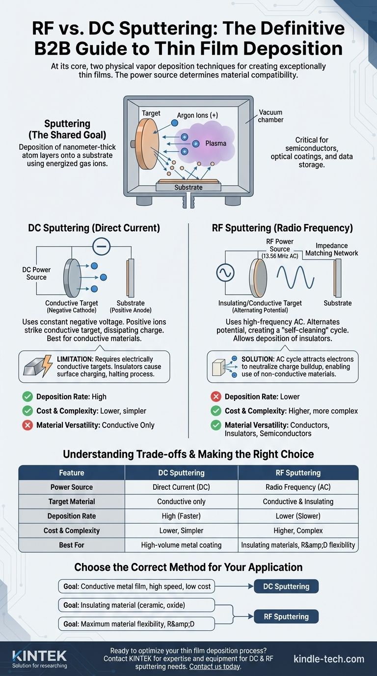
At its core, DC and RF sputtering are two physical vapor deposition techniques used to create exceptionally thin films of material on a surface. The fundamental difference between them is the type of electrical power source used, which directly determines what kind of material you can deposit. DC (Direct Current) sputtering is used for electrically conductive materials, while RF (Radio Frequency) sputtering is necessary for non-conductive, insulating materials.
The choice between DC and RF sputtering is dictated almost entirely by the electrical conductivity of your target material. DC sputtering is faster and cheaper but only works for conductive targets, while RF sputtering prevents charge buildup on insulating targets, making it more versatile but also slower and more expensive.
The Shared Goal: Thin Film Deposition
What is Sputtering?
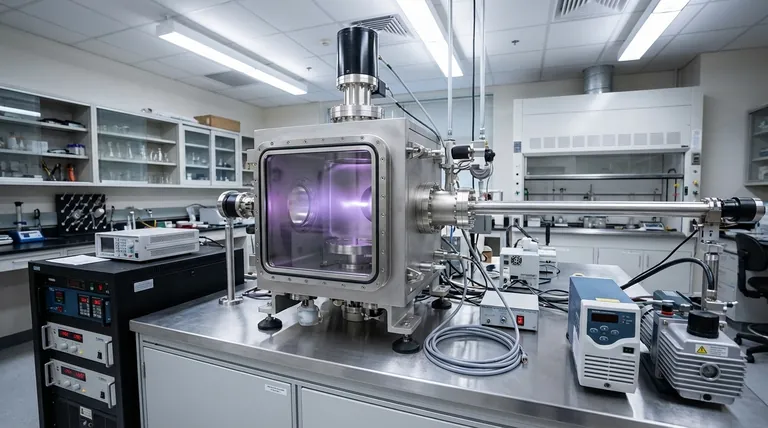
Sputtering is a process performed in a vacuum chamber to deposit a thin layer of atoms, often just nanometers thick, onto a substrate.
It involves bombarding a source material, known as the target, with energized gas ions (typically Argon). This collision has enough force to knock atoms loose from the target's surface. These ejected atoms then travel through the chamber and coat the substrate, forming a uniform thin film.
This technique is critical in manufacturing semiconductors, optical coatings, and data storage devices like disk drives.
The Mechanism of DC Sputtering
How It Works
DC sputtering uses a Direct Current (DC) power source. The target material is set up as the cathode (negative electrode), and the substrate is placed on the anode (positive electrode).
The constant negative voltage on the target attracts the positively charged gas ions. These ions accelerate towards the target and collide with it, dislodging atoms for deposition.
The Critical Limitation: Conductivity
This process works efficiently only if the target material is electrically conductive. The target must be able to dissipate the positive charge from the impacting ions to maintain its negative potential.
If you attempt to use an insulating target, the positive ions accumulate on its surface. This buildup of charge, known as surface charging, quickly neutralizes the target's negative voltage, repels incoming ions, and halts the sputtering process entirely.
How RF Sputtering Solves the Insulator Problem
The Alternating Current Solution
RF sputtering overcomes the limitation of DC sputtering by using a high-frequency Alternating Current (AC) power source, typically operating at 13.56 MHz.
Instead of a constant negative voltage, the electrical potential on the target rapidly alternates between negative and positive.
The Self-Cleaning Cycle
This rapid alternation creates a "self-cleaning" effect in two distinct half-cycles.
During the longer, negative portion of the cycle, positive ions are attracted to bombard the target and sputter atoms, just as in the DC process.
During the brief, positive portion of the cycle, the target attracts a shower of electrons from the plasma. These electrons instantly neutralize any excess positive charge that has accumulated on the surface.
Unlocking New Materials
By continuously clearing the positive ion buildup, RF sputtering allows for the sustained deposition of non-conductive (insulating or dielectric) materials, such as ceramics and oxides, which is impossible with a standard DC setup.
Understanding the Trade-offs
Deposition Rate
DC sputtering is significantly faster. The power is delivered to the target more efficiently, resulting in a higher rate of material deposition compared to RF sputtering.
Cost and Complexity
DC systems are simpler and more economical. They require a straightforward DC power supply. RF systems are more complex and expensive, as they need a high-frequency AC generator and an impedance matching network to operate efficiently.
Material Versatility
RF sputtering is far more versatile. While DC is limited to conductive metals and compounds, RF can deposit virtually any material, including conductors, insulators, and semiconductors.
Process Scale
Due to its speed and cost-efficiency, DC sputtering is often preferred for large-scale production and coating large substrates. RF sputtering is more commonly used for smaller substrates or in research and development where material flexibility is paramount.
Making the Right Choice for Your Application
Choosing the correct method is a direct consequence of your material requirements and operational goals.
- If your primary focus is depositing a conductive metal film with high speed and low cost: DC sputtering is the clear and superior choice.
- If your primary focus is depositing an insulating material like a ceramic or oxide: RF sputtering is the necessary and correct technique.
- If your primary focus is maximum material flexibility in a research or lab setting: An RF system provides the versatility to handle any type of target material you may need.
Ultimately, understanding how each method handles electrical charge is the key to selecting the correct sputtering technique for your material.
Summary Table:
| Feature | DC Sputtering | RF Sputtering |
|---|---|---|
| Power Source | Direct Current (DC) | Radio Frequency (AC) |
| Target Material | Conductive materials only | Both conductive and insulating materials |
| Deposition Rate | High | Lower |
| Cost & Complexity | Lower cost, simpler setup | Higher cost, more complex |
| Best For | High-volume metal coating | Insulating materials, R&D flexibility |
Ready to optimize your thin film deposition process? Whether you're coating conductive metals with DC sputtering or working with insulating ceramics using RF sputtering, KINTEK has the expertise and equipment to meet your laboratory's unique needs. Our range of sputtering systems ensures precision, efficiency, and reliability for semiconductors, optical coatings, and more. Contact us today to discuss your project and discover how KINTEK can enhance your lab's capabilities!
Visual Guide
Related Products
- Three-dimensional electromagnetic sieving instrument
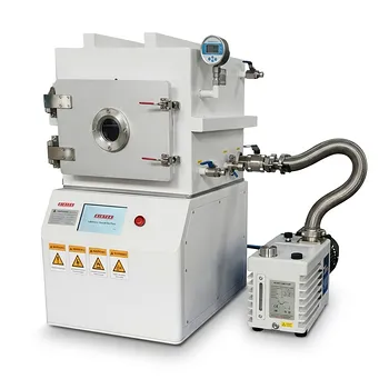
- Chemical Vapor Deposition CVD Equipment System Chamber Slide PECVD Tube Furnace with Liquid Gasifier PECVD Machine
- Customer Made Versatile CVD Tube Furnace Chemical Vapor Deposition Chamber System Equipment
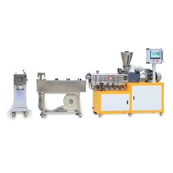
- Twin Screw Extruder Plastic Granulation Machine
- HFCVD Machine System Equipment for Drawing Die Nano-Diamond Coating
People Also Ask
- What is the advantage of sieving? A Simple, Reliable Method for Particle Size Analysis
- What are advantages and disadvantages of sieving method? A Guide to Reliable & Cost-Effective Particle Sizing
- What are the precautions for sieving method? Ensure Accurate Particle Size Analysis
- What are the limitations of sieving? Understanding the Constraints of Particle Size Analysis
- What is sieving and how does it work? A Guide to Accurate Particle Size Analysis