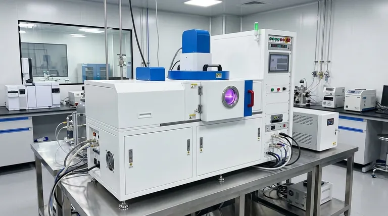
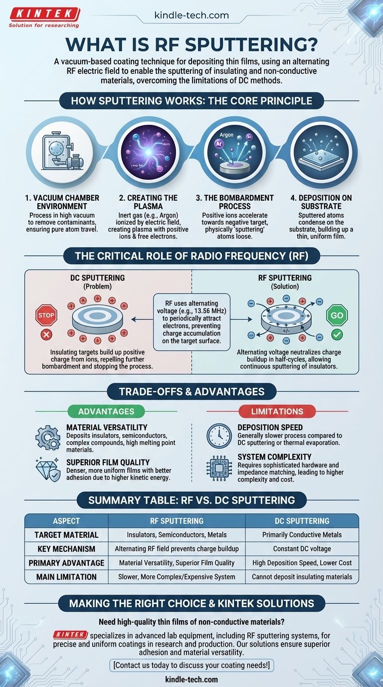
At its core, RF sputtering is a vacuum-based coating technique used to deposit extremely thin films of material onto a surface. It works by bombarding a source material (the "target") with ionized gas in a plasma, physically knocking atoms loose so they can settle on a substrate. The key differentiator of RF (Radio Frequency) sputtering is its use of an alternating electric field, which makes it uniquely capable of depositing insulating, or non-conductive, materials.
While all sputtering techniques physically eject atoms from a target to coat a substrate, RF sputtering specifically solves the problem of electrical charge buildup. This allows it to deposit high-quality films of non-metallic materials like ceramics and oxides, a task that simpler methods like DC sputtering cannot perform.
How Sputtering Works: The Core Principle
To understand the specific advantage of RF, we must first understand the general process of sputter deposition, which is a form of Physical Vapor Deposition (PVD).
The Vacuum Chamber Environment
The entire process takes place inside a high-vacuum chamber. Removing air and other particles is critical to ensure the sputtered atoms can travel from the target to the substrate without colliding with contaminants.
Creating the Plasma
An inert gas, most commonly argon, is introduced into the chamber at low pressure. A strong electric field is applied, which strips electrons from the argon atoms, creating a glowing, ionized gas known as a plasma. This plasma consists of positively charged argon ions and free electrons.
The Bombardment Process
The target material, which serves as the cathode, is given a negative electrical potential. This attracts the positively charged argon ions from the plasma, which accelerate towards the target at high speeds.
These energetic ions act like atomic-scale sandblasters, crashing into the target and transferring their momentum. This collision physically ejects, or "sputters", individual atoms from the target material.
Deposition on the Substrate
The ejected target atoms travel through the vacuum chamber and condense on the substrate (the object being coated), gradually building up a thin, uniform film.
The Critical Role of Radio Frequency (RF)
The simple process described above works perfectly for conductive targets, like metals. However, it fails completely for insulating targets. This is where RF becomes essential.
The Problem with Insulating Targets
If you use a constant negative voltage (Direct Current, or DC) with an insulating target (like a ceramic), the positive argon ions that strike its surface have nowhere to go. Their positive charge accumulates on the target surface.
This buildup of positive charge quickly neutralizes the negative potential of the cathode, effectively creating an electrical shield that repels any more incoming argon ions. The sputtering process stops almost immediately.
The RF Solution: Alternating the Voltage
RF sputtering solves this by replacing the constant DC voltage with an alternating radio frequency voltage (typically 13.56 MHz). This field rapidly flips its polarity millions of times per second.
In the first half of the cycle, the target is negative, attracting argon ions for bombardment and sputtering just like in the DC process.
In the second half-cycle, the target briefly becomes positive. During this phase, it attracts the highly mobile electrons from the plasma, which flood the surface and neutralize the positive charge that built up during the sputtering phase. This "resets" the target surface, allowing the sputtering process to continue indefinitely.
Understanding the Trade-offs and Advantages
RF sputtering is a powerful tool, but it's important to understand where it excels and what its limitations are.
Key Advantage: Material Versatility
The primary reason to use RF sputtering is its ability to deposit virtually any material, including insulators, semiconductors, and complex compounds that cannot be handled by DC sputtering. It is also excellent for depositing materials with very high melting points and alloys that are difficult to process with other methods.
Key Advantage: Superior Film Quality
Sputtered atoms have significantly higher kinetic energy than those from thermal evaporation. This results in films that are denser, more uniform, and have far better adhesion to the substrate.
Main Limitation: Deposition Speed
Generally, RF sputtering is a slower process compared to DC sputtering or thermal evaporation techniques. The time required to deposit a film of a certain thickness is often longer.
Main Limitation: System Complexity
RF power systems require more sophisticated hardware, including an impedance matching network to efficiently transfer power to the plasma. This makes RF sputtering systems more complex and expensive than their DC counterparts.
Making the Right Deposition Choice
Selecting the correct deposition method depends entirely on your material and project goals.
- If your primary focus is depositing conductive materials (metals) quickly: DC magnetron sputtering is often a more cost-effective and faster choice.
- If your primary focus is depositing non-conductive materials (ceramics, oxides, polymers): RF sputtering is the essential and industry-standard solution.
- If your primary focus is maximum film quality, density, and adhesion for any material type: RF sputtering provides superior results compared to simpler methods like thermal evaporation.
Ultimately, choosing RF sputtering is about enabling the high-precision deposition of materials that would otherwise be impossible to work with.
Summary Table:
| Aspect | RF Sputtering | DC Sputtering |
|---|---|---|
| Target Material | Insulators, Semiconductors, Metals | Primarily Conductive Metals |
| Key Mechanism | Alternating RF field prevents charge buildup | Constant DC voltage |
| Primary Advantage | Material Versatility, Superior Film Quality | High Deposition Speed, Lower Cost |
| Main Limitation | Slower, More Complex/Expensive System | Cannot deposit insulating materials |
Need to deposit high-quality thin films of non-conductive materials?
KINTEK specializes in advanced lab equipment, including RF sputtering systems, to help you achieve precise and uniform coatings for your research or production needs. Our solutions are designed for laboratories requiring superior film adhesion and material versatility.
Contact us today to discuss how our sputtering technology can enhance your coating processes!
Visual Guide
Related Products
- RF PECVD System Radio Frequency Plasma-Enhanced Chemical Vapor Deposition RF PECVD
- Spark Plasma Sintering Furnace SPS Furnace
- Horizontal High Temperature Graphite Vacuum Graphitization Furnace
People Also Ask
- What is plasma CVD? Unlock Low-Temperature Thin Film Deposition for Sensitive Materials
- What is an example of PECVD? RF-PECVD for High-Quality Thin Film Deposition
- What is plasma enhanced chemical vapour deposition PECVD used for? Enable Low-Temp Thin Films for Electronics & Solar
- What is plasma enhanced chemical Vapour deposition process used for fabrication of? A Guide to Low-Temperature Thin Films
- What is plasma chemical vapor deposition? A Low-Temperature Thin Film Coating Solution


