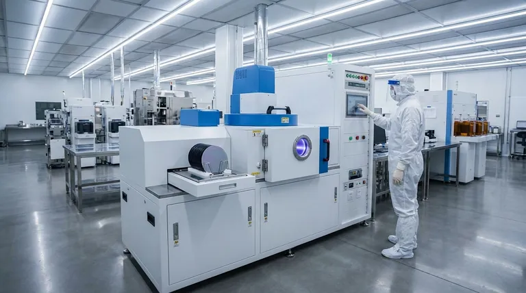
In semiconductor manufacturing, sputter deposition is a high-precision process used to apply ultra-thin films of material onto a silicon wafer. It operates by bombarding a source material, known as a target, with energetic ions in a vacuum. This impact physically knocks atoms off the target, which then travel and condense onto the wafer, forming a perfectly uniform and pure coating.
At its core, sputter deposition is less like spraying paint and more like a controlled, atomic-scale sandblasting. It uses physical momentum, not heat, to move material, giving manufacturers exceptional control over the thickness, purity, and quality of the layers that form an integrated circuit.
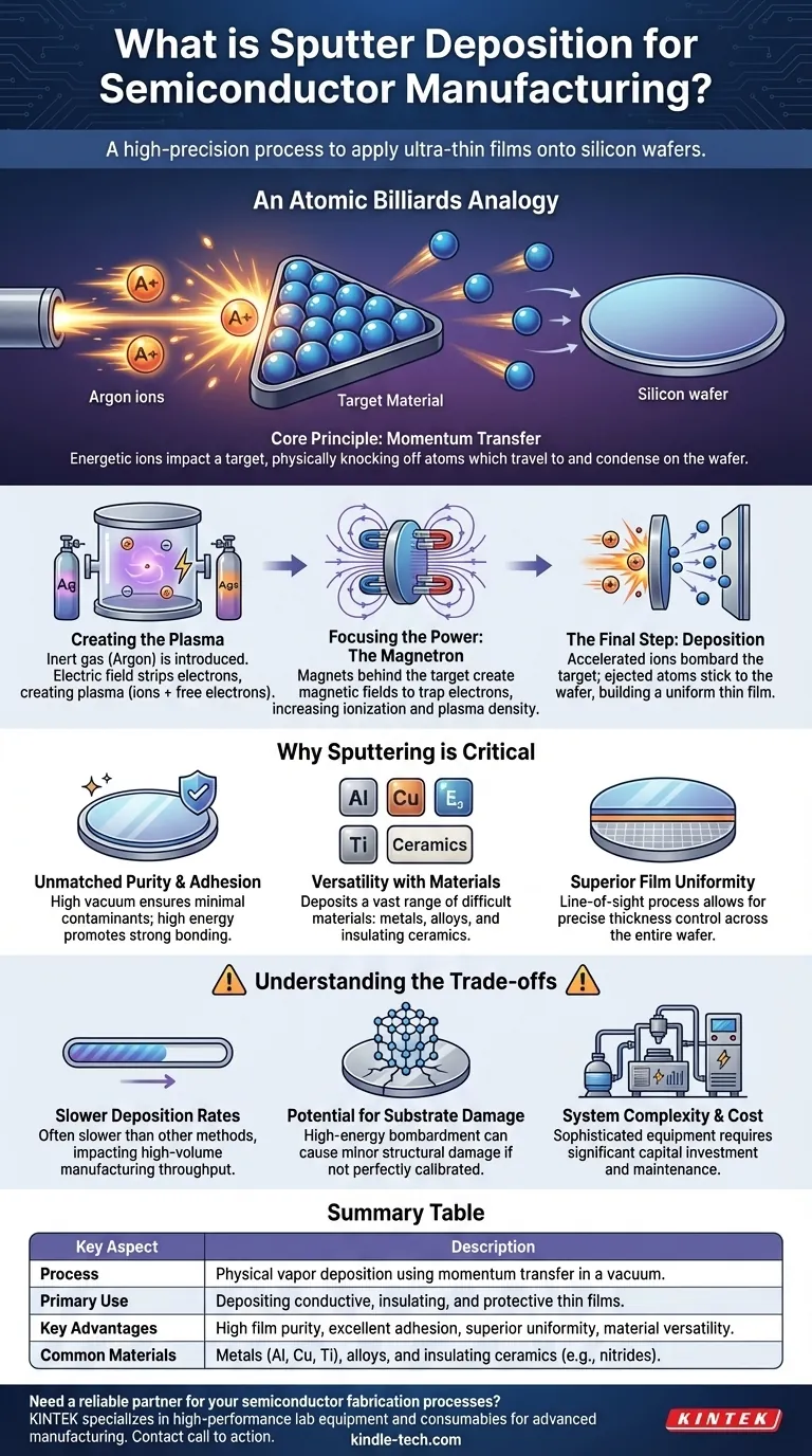
How Sputter Deposition Works: An Atomic Billiards Analogy
To understand sputtering, it is essential to move away from concepts like melting or chemical reactions. The process is entirely mechanical, driven by momentum transfer between individual atoms in a highly controlled environment.
The Core Principle: Momentum Transfer
Sputtering relies on a simple principle of physics. Imagine a tightly packed rack of billiard balls (the target material).
You then fire the cue ball (an energetic ion) into the rack. The impact transfers momentum, causing balls to fly off in various directions. In sputtering, these ejected "balls" are individual atoms that travel until they strike the wafer.
Creating the Ions: The Plasma
The "cue balls" are created by introducing an inert gas, typically Argon, into a vacuum chamber.
An electric field is applied, which strips electrons from the Argon atoms. This creates a plasma, a cloud of positively charged Argon ions and free electrons.
Focusing the Power: The Magnetron
Modern systems use powerful magnets behind the target material in a configuration called a magnetron.
This magnetic field traps electrons near the target's surface. These trapped electrons travel a much longer, spiral path, drastically increasing the probability that they will collide with and ionize more Argon atoms, creating a dense, efficient plasma right where it's needed.
The Final Step: Deposition
The positively charged Argon ions are accelerated by the electric field and slam into the negatively charged target.
Atoms ejected from the target travel through the vacuum and stick to the substrate (the silicon wafer), gradually building a thin film with exceptional uniformity.
Why Sputtering is Critical for Modern Electronics
Sputtering is not just one of many options; it is a foundational technology in chip fabrication because of the unique advantages it offers for building microscopic structures.
Unmatched Purity and Adhesion
Because the entire process occurs in a high vacuum, there are virtually no contaminants to get trapped in the film. The high kinetic energy of the sputtered atoms also helps them bond tightly to the wafer surface, creating highly durable and reliable layers.
Versatility with Materials
Sputtering can deposit a vast range of materials that are otherwise difficult to work with. This includes pure metals for electrical contacts (like aluminum or copper), complex alloys, and insulating ceramic materials for protective coatings.
Superior Film Uniformity
The line-of-sight, controlled nature of the process allows for the creation of films with exceptionally precise thickness across the entire diameter of a wafer. This uniformity is non-negotiable for ensuring that all chips produced from a single wafer perform identically.
Understanding the Trade-offs and Limitations
While powerful, sputtering is a specialized process with specific constraints that engineers must manage. Trustworthy analysis requires acknowledging its limitations.
Slower Deposition Rates
Compared to thermal evaporation or chemical vapor deposition (CVD), sputtering can be a slower process. The rate of film growth is often measured in angstroms or nanometers per minute, making throughput a key consideration for high-volume manufacturing.
Potential for Substrate Damage
The high-energy bombardment that makes the process work can, if not perfectly calibrated, cause minor structural damage to the delicate crystal lattice of the underlying silicon wafer. This is a constant focus of process control and optimization.
System Complexity and Cost
Sputtering systems are sophisticated and expensive pieces of equipment. They require high-vacuum pumps, powerful magnets, precise gas handling, and high-voltage power supplies, all of which demand significant capital investment and maintenance.
Making the Right Choice for Your Goal
Sputtering is chosen to solve specific problems in the complex recipe of chip manufacturing. Its application is always tied to a precise engineering goal.
- If your primary focus is creating conductive pathways: Sputtering is the industry standard for depositing the metal layers (e.g., aluminum, copper, titanium) used for contacts, interconnects, and wiring.
- If your primary focus is device protection and reliability: Sputtering is used to apply durable, chemically resistant films like nitrides that encapsulate and protect the sensitive components on the chip.
- If your primary focus is building complex material stacks: Sputtering allows for the deposition of multiple, distinct layers of different materials in sequence without breaking vacuum, enabling the creation of advanced device structures.
Ultimately, sputter deposition provides the atomic-level control required to build the complex, multi-layered structures that define modern integrated circuits.
Summary Table:
| Key Aspect | Description |
|---|---|
| Process | Physical vapor deposition using momentum transfer in a vacuum. |
| Primary Use | Depositing conductive, insulating, and protective thin films on wafers. |
| Key Advantages | High film purity, excellent adhesion, superior uniformity, material versatility. |
| Common Materials | Metals (Al, Cu, Ti), alloys, and insulating ceramics (e.g., nitrides). |
Need a reliable partner for your semiconductor fabrication processes?
KINTEK specializes in high-performance lab equipment and consumables for advanced manufacturing. Whether you are developing next-generation chips or optimizing your production line, our sputtering targets and deposition systems are engineered for precision, purity, and repeatability.
Let us help you achieve superior thin-film results. Contact our experts today to discuss your specific semiconductor manufacturing needs.
Visual Guide
Related Products
- Chemical Vapor Deposition CVD Equipment System Chamber Slide PECVD Tube Furnace with Liquid Gasifier PECVD Machine
- HFCVD Machine System Equipment for Drawing Die Nano-Diamond Coating
- Customer Made Versatile CVD Tube Furnace Chemical Vapor Deposition Chamber System Equipment
- Inclined Rotary Plasma Enhanced Chemical Vapor Deposition PECVD Equipment Tube Furnace Machine
- Inclined Rotary Plasma Enhanced Chemical Vapor Deposition PECVD Equipment Tube Furnace Machine
People Also Ask
- What are the advantages of chemical vapor deposition? Achieve Superior Thin Films for Your Lab
- What are the core advantages of PE-CVD in OLED encapsulation? Protect Sensitive Layers with Low-Temp Film Deposition
- What is plasma enhanced chemical vapor deposition PECVD equipment? A Guide to Low-Temperature Thin Film Deposition
- What is the chemical vapor deposition growth process? Build Superior Thin Films from the Atom Up
- How are carbon nanotubes grown? Master Scalable Production with Chemical Vapor Deposition


