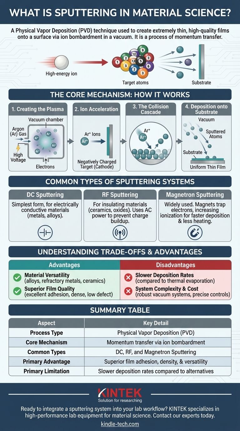
In material science, sputtering is a physical vapor deposition (PVD) technique used to create extremely thin, high-quality films of material onto a surface. It works by bombarding a solid source material, known as a "target," with energetic ions in a vacuum. This collision physically ejects or "sputters" atoms from the target, which then travel and deposit onto a nearby object, or "substrate," forming a uniform coating.
At its core, sputtering is a process of momentum transfer, not a chemical or thermal one. Imagine it as a microscopic game of billiards: a high-energy "cue ball" (an ion) strikes a rack of "billiard balls" (target atoms), knocking them out and sending them flying toward the substrate.

The Core Mechanism: How Sputtering Works
To understand sputtering's value, you must first grasp its fundamental steps. The entire process takes place inside a sealed vacuum chamber to ensure the purity of the deposited film.
Step 1: Creating the Plasma
The process begins by introducing a small, controlled amount of an inert gas, almost always Argon (Ar), into the vacuum chamber.
A high voltage is then applied, which strips electrons from the Argon atoms. This creates a plasma, an ionized gas consisting of positive Argon ions (Ar+) and free electrons, which is often visible as a characteristic glow.
Step 2: Ion Acceleration
The target material (the substance you want to deposit) is set up as a cathode, meaning it is given a strong negative electrical charge.
The positively charged Argon ions in the plasma are naturally accelerated with great force toward this negatively charged target.
Step 3: The Collision Cascade
When the high-energy Argon ion strikes the target surface, it transfers its momentum to the target's atoms.
This collision sets off a chain reaction, dislodging target atoms and ejecting them from the surface. This physical ejection is the "sputtering" effect.
Step 4: Deposition onto the Substrate
The dislodged atoms from the target travel through the low-pressure environment of the chamber.
They eventually strike the substrate (the object to be coated), where they condense and build up, layer by layer, to form a thin, dense, and highly uniform film.
Common Types of Sputtering Systems
While the principle remains the same, different sputtering technologies have been developed to handle various materials and improve efficiency.
DC Sputtering
Direct Current (DC) sputtering is the simplest form. It uses a DC voltage source and is highly effective for depositing electrically conductive materials like pure metals and alloys. It cannot, however, be used for insulating materials.
RF Sputtering
Radio Frequency (RF) sputtering is the solution for non-conductive, insulating materials like ceramics and oxides. It uses an AC power source that alternates at radio frequencies.
This rapid switching prevents a positive charge buildup on the insulator's surface, which would otherwise repel the Argon ions and halt the sputtering process.
Magnetron Sputtering
This is the most widely used method in industry. Magnetron sputtering places powerful magnets behind the target.
These magnets trap electrons from the plasma close to the target's surface, dramatically increasing the number of Argon atoms that become ionized. This results in a denser plasma, which leads to much faster deposition rates and less heating of the substrate.
Understanding the Trade-offs and Advantages
No single technique is perfect for every application. Sputtering has distinct advantages but also comes with limitations that are important to recognize.
Advantage: Material Versatility
Sputtering can deposit a vast range of materials, including complex alloys, refractory metals, and (with RF) ceramics and compounds. The composition of the sputtered film is very close to the composition of the target.
Advantage: Superior Film Quality
Sputtered films are renowned for their excellent adhesion to the substrate. They are typically very dense, have a low defect count, and offer precise, repeatable control over film thickness.
Disadvantage: Slower Deposition Rates
Generally, sputtering deposits material more slowly than other methods like thermal evaporation. For high-volume, low-cost applications, this can be a significant drawback.
Disadvantage: System Complexity and Cost
Sputtering systems are mechanically complex and more expensive than simpler deposition techniques. They require robust vacuum systems, high-voltage power supplies, and precise gas flow control.
Making the Right Choice for Your Application
Selecting the correct deposition method depends entirely on the material properties you need to achieve for your final product.
- If your primary focus is high-purity, dense films with excellent adhesion: Sputtering is often the superior choice, especially for complex alloys or coatings that must withstand wear.
- If you need to deposit insulating materials like ceramics or oxides: RF sputtering is the industry-standard and most reliable method available.
- If your goal is high-speed deposition of simple metals on a tight budget: You may want to evaluate thermal evaporation as a potentially more cost-effective alternative.
Ultimately, understanding the physical principles of sputtering empowers you to create materials with the precise performance characteristics your project demands.
Summary Table:
| Aspect | Key Detail |
|---|---|
| Process Type | Physical Vapor Deposition (PVD) |
| Core Mechanism | Momentum transfer via ion bombardment |
| Common Types | DC, RF, and Magnetron Sputtering |
| Primary Advantage | Superior film adhesion, density, and material versatility |
| Primary Limitation | Slower deposition rates compared to some alternatives |
Ready to integrate a sputtering system into your lab workflow? KINTEK specializes in high-performance lab equipment and consumables for material science. Our sputtering systems are designed to deliver the precise, high-quality thin films your research or production demands. Contact our experts today to discuss how we can support your laboratory's specific coating needs.
Visual Guide
Related Products
- Spark Plasma Sintering Furnace SPS Furnace
- Vacuum Induction Melting Spinning System Arc Melting Furnace
- Chemical Vapor Deposition CVD Equipment System Chamber Slide PECVD Tube Furnace with Liquid Gasifier PECVD Machine
- Customer Made Versatile CVD Tube Furnace Chemical Vapor Deposition Chamber System Equipment
People Also Ask
- What is the difference between spark plasma sintering and flash sintering? A Guide to Advanced Sintering Methods
- Why are Spark Plasma Sintering (SPS) furnaces or hot presses utilized in the preparation of Li3PS4 solid electrolytes?
- What is SPS sintering method? A Guide to High-Speed, High-Performance Material Fabrication
- What is the process fundamentals of spark plasma sintering? Achieve Rapid, High-Density Material Consolidation
- What is the theory of spark plasma sintering? A Guide to Rapid, Low-Temperature Densification


