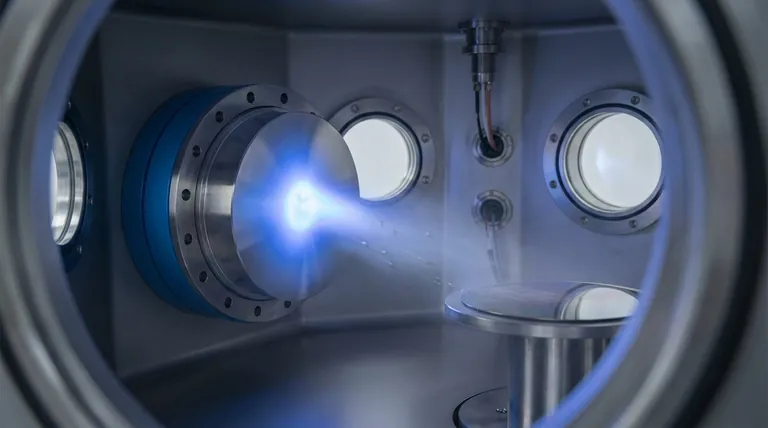
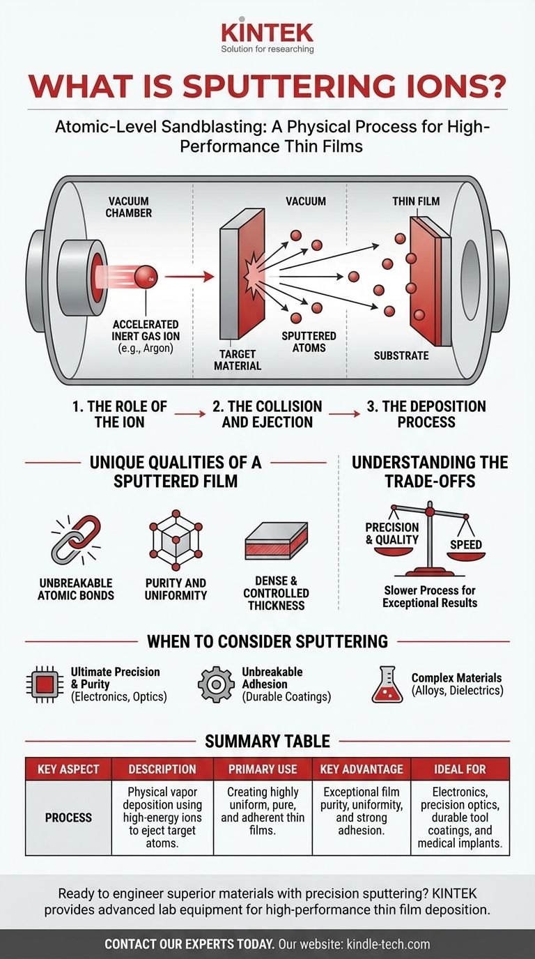
In essence, sputtering is a physical process where high-energy ions bombard a solid material, knocking atoms loose from its surface. These ejected atoms then travel and deposit onto a nearby object, forming an exceptionally thin and uniform coating. This technique, also known as Ion Beam Deposition (IBD), is fundamental to manufacturing high-performance materials in fields like electronics and optics.
The core concept to grasp is that sputtering is not a chemical reaction. It is a purely physical, "atomic-level sandblasting" that allows for the controlled transfer of material from a source target to a final product, one atom at a time.
The Core Mechanism: How Sputtering Works
To understand the value of sputtering, you must first visualize the physics at play. The process is a chain of cause and effect, starting with an accelerated ion and ending with a deposited atom.
The Role of the Ion
The process begins with an ion, typically from an inert gas like argon. This ion is given a high amount of kinetic energy by accelerating it in an electric field.
It acts as a projectile, aimed at a block of the material you wish to deposit, which is called the target. The ion's purpose is simply to carry and deliver energy.
The Collision and Ejection
When the high-energy ion strikes the target material, it transfers its momentum and energy to the atoms within the target's surface.
This energy transfer is like a powerful billiard break. If an atom on the surface receives enough energy from the collision, it can overcome its atomic bonds and be physically ejected, or sputtered, from the target. These ejected particles are typically neutral atoms, not ions.
The Deposition Process
These newly freed atoms travel through a vacuum chamber and land on a nearby surface, known as the substrate.
As millions of these atoms land on the substrate, they build up layer-by-layer, forming a new, extremely thin film. Because the process is so controlled, the resulting film is highly uniform and dense.
The Unique Qualities of a Sputtered Film
The "why" behind sputtering lies in the unparalleled quality of the films it produces. The physical nature of the deposition process imparts unique and highly desirable characteristics.
Unbreakable Atomic Bonds
The reference to a "virtually unbreakable" bond is not an exaggeration. The sputtered atoms arrive at the substrate with significant kinetic energy, which helps them form a dense, tightly packed structure with extremely strong adhesion to the surface.
Purity and Uniformity
Because sputtering happens in a vacuum and uses an inert gas, the risk of contamination is exceptionally low. This results in a very pure film.
Furthermore, the process can be finely controlled to ensure the film's thickness is uniform across the entire substrate, which is critical for applications like optical lenses and semiconductor wafers.
Understanding the Trade-offs
No technical process is without its compromises. While powerful, sputtering has practical considerations that define when it is the right choice.
Precision vs. Speed
Building a film one atomic layer at a time is an inherently slow process. The exceptional precision and quality of sputtered films often come at the cost of deposition speed.
For applications where thick coatings are needed quickly and absolute uniformity is not critical, other methods like thermal evaporation or chemical vapor deposition might be more suitable.
The Meaning of "Cost-Effective"
Sputtering is considered cost-effective for applications where its unique benefits are a requirement. The equipment is complex, but the ability to create highly durable, pure, and uniform films from almost any material often justifies the investment.
The cost is relative to the high-value performance of the final product. It is not a "cheap" process in absolute terms but provides value that is difficult to achieve otherwise.
When to Consider Sputtering for Your Project
Choosing a deposition method depends entirely on your end goal. The decision to use sputtering hinges on whether you need the specific qualities it delivers.
- If your primary focus is ultimate film precision and purity: Sputtering is the gold standard for creating highly uniform, dense films for demanding applications like precision optics or semiconductor devices.
- If your primary focus is unbreakable adhesion: The energetic nature of the process ensures the deposited film bonds exceptionally well, making it ideal for durable, hard coatings on tools or medical implants.
- If your primary focus is depositing a complex or specialized material: Because it is a physical process, sputtering can deposit a vast range of materials, including metals, alloys, and dielectrics, that are challenging for chemical-based methods.
By understanding the mechanics of sputtering, you can better leverage its power to engineer materials at the atomic scale.
Summary Table:
| Key Aspect | Description |
|---|---|
| Process | Physical vapor deposition using high-energy ions to eject target atoms. |
| Primary Use | Creating highly uniform, pure, and adherent thin films. |
| Key Advantage | Exceptional film purity, uniformity, and strong adhesion. |
| Ideal For | Electronics, precision optics, durable tool coatings, and medical implants. |
Ready to engineer superior materials with precision sputtering?
KINTEK specializes in providing the advanced lab equipment and consumables needed for high-performance thin film deposition. Whether you are developing semiconductor devices, precision optics, or durable coatings, our expertise ensures you achieve the ultimate in film purity, uniformity, and adhesion.
Contact our experts today to discuss how our solutions can accelerate your R&D and production.
Visual Guide
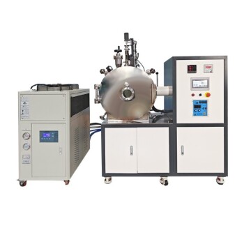
Related Products
- RF PECVD System Radio Frequency Plasma-Enhanced Chemical Vapor Deposition RF PECVD
- Chemical Vapor Deposition CVD Equipment System Chamber Slide PECVD Tube Furnace with Liquid Gasifier PECVD Machine
- Split Chamber CVD Tube Furnace with Vacuum Station Chemical Vapor Deposition System Equipment Machine
- VHP Sterilization Equipment Hydrogen Peroxide H2O2 Space Sterilizer
- Lab-Scale Vacuum Induction Melting Furnace
People Also Ask
- How are PECVD and CVD different? A Guide to Choosing the Right Thin-Film Deposition Process
- What is an example of PECVD? RF-PECVD for High-Quality Thin Film Deposition
- What are the benefits of PECVD? Achieve Superior Low-Temperature Thin Film Deposition
- What are the applications of PECVD? Essential for Semiconductors, MEMS, and Solar Cells
- What is the principle of plasma enhanced chemical vapor deposition? Achieve Low-Temperature Thin Film Deposition