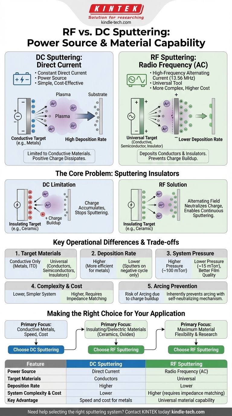
At its core, the difference between RF and DC sputtering lies in the power source, a distinction that directly determines the types of materials you can deposit. RF (Radio Frequency) sputtering uses a high-frequency alternating current (AC), while DC (Direct Current) sputtering uses a constant direct current. This makes RF sputtering a universal tool for both conductive and insulating materials, whereas DC sputtering is restricted to depositing materials that can conduct electricity.
The choice between RF and DC sputtering is not about which method is "better," but which is appropriate for your target material. DC sputtering is a simpler, often faster method for conductive metals, while RF sputtering's alternating field is essential to overcome charge buildup when depositing non-conductive, insulating materials.
The Core Problem: Sputtering Insulating Materials
The need for RF sputtering arose from a fundamental limitation in the DC sputtering process. Understanding this limitation is key to grasping the difference.
The DC Sputtering Limitation: Positive Charge Buildup
In DC sputtering, a constant, high-voltage negative charge is applied to the target material you wish to deposit. This negatively charged target attracts positively charged ions (typically argon) from the plasma.
These ions strike the target with enough force to physically knock atoms off its surface—this is the "sputtering" process. The dislodged atoms then travel and coat your substrate.
This works perfectly for conductive targets, like metals, because the target can dissipate the positive charge from the impacting ions. However, if the target is an insulator (like a ceramic or oxide), it cannot conduct electricity. Positive charge from the ions rapidly accumulates on the target surface, neutralizing the negative potential and repelling any more positive ions, effectively stopping the sputtering process.
The RF Sputtering Solution: Alternating the Field
RF sputtering solves this problem by using an alternating current, typically at an industry-standard frequency of 13.56 MHz. The electrical potential of the target rapidly switches between negative and positive millions of times per second.
During the negative half-cycle, the target behaves like a DC target, attracting positive ions and sputtering atoms. This is when deposition occurs.
During the much shorter positive half-cycle, the target attracts a flood of mobile electrons from the plasma. These electrons instantly neutralize the positive charge that built up on the insulating surface, "resetting" it for the next sputtering cycle. This constant charge neutralization is what allows for the continuous sputtering of any material.
Key Operational Differences
The underlying physics of the power source creates several practical differences in how these two systems operate.
Target Materials: The Deciding Factor
This is the most critical distinction.
- DC Sputtering: Only effective for electrically conductive materials, such as most metals and transparent conductive oxides like ITO.
- RF Sputtering: Universal. It can deposit conductors, semiconductors, and insulators (dielectrics), making it essential for ceramics, oxides, and other non-conductive compounds.
Deposition Rate
For a given conductive material that can be sputtered by either method, DC sputtering generally offers a higher deposition rate.
This is because sputtering in an RF system only occurs during the negative portion of the AC cycle. DC sputtering, by contrast, is "always on," leading to a faster and more efficient process for metals.
System Pressure and Plasma
RF sputtering can sustain a stable plasma at a lower operating pressure (often below 15 mTorr) compared to DC sputtering (which may require up to 100 mTorr).
Lower pressure reduces the chance of sputtered atoms colliding with gas molecules on their way to the substrate. This creates a more direct, "line-of-sight" deposition path, which can improve the density and quality of the final thin film.
Understanding the Trade-offs
Choosing a sputtering technique involves balancing capability against complexity and cost.
Complexity and Cost
DC sputtering systems are mechanically and electronically simpler. A high-voltage DC power supply is relatively straightforward, making the overall system less expensive and easier to maintain.
RF sputtering systems are more complex. They require a dedicated RF generator and an impedance matching network—a critical component that fine-tunes the electrical load to ensure maximum power is transferred to the plasma, not reflected back to the source. This added complexity increases the system's cost.
Speed vs. Versatility
The central trade-off is clear:
- DC offers speed and cost-effectiveness but is limited to conductive targets.
- RF offers universal material versatility but at the cost of lower deposition rates and higher system complexity.
Preventing Arcing
In DC systems, the charge buildup on any insulating patches or contaminants on a target can lead to a sudden, damaging electrical discharge known as arcing. RF sputtering's self-neutralizing mechanism inherently prevents this type of charge accumulation, resulting in a more stable plasma and protecting the target from damage.
Making the Right Choice for Your Application
Your decision ultimately hinges on the material you need to deposit and your operational priorities.
- If your primary focus is depositing conductive metals quickly and cost-effectively: DC sputtering is almost always the superior choice.
- If your primary focus is depositing insulating or dielectric materials (like ceramics or oxides): RF sputtering is the necessary and standard method.
- If your primary focus is maximum material flexibility in a research environment: RF sputtering provides the versatility to work with any type of target material.
Understanding this core distinction in charge management empowers you to select the precise tool for your thin-film deposition goal.
Summary Table:
| Feature | DC Sputtering | RF Sputtering |
|---|---|---|
| Power Source | Direct Current (DC) | Radio Frequency (AC) |
| Target Materials | Conductors (Metals, ITO) | Conductors, Semiconductors, Insulators |
| Deposition Rate | Higher for conductors | Lower |
| System Complexity & Cost | Lower | Higher (requires impedance matching) |
| Key Advantage | Speed and cost for metals | Universal material capability |
Need help selecting the right sputtering system for your lab's unique materials?
Whether you are depositing conductive metals or complex insulating ceramics, choosing the correct sputtering method is critical for your research and production outcomes. KINTEK specializes in providing high-quality lab equipment, including sputtering systems, to meet your specific thin-film deposition needs.
Let our experts guide you to the optimal solution. Contact us today to discuss your application and discover how KINTEK can enhance your laboratory's capabilities!
Visual Guide