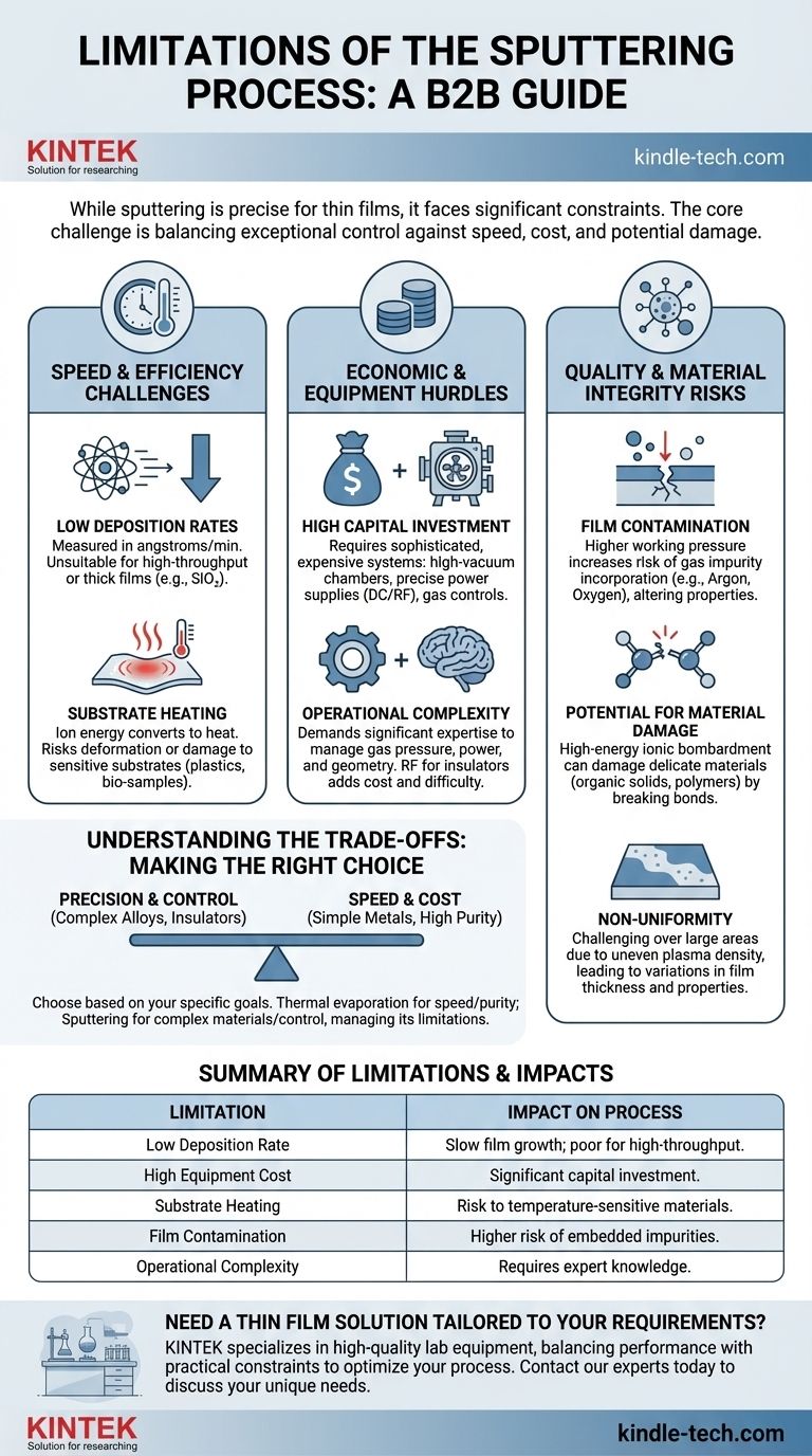
While sputtering is a highly versatile and precise method for creating thin films, it is constrained by several significant limitations. The primary drawbacks are its relatively low deposition speed, the high cost and complexity of the required equipment, the potential for heat-related damage to the substrate, and a greater risk of film contamination compared to other vacuum deposition techniques.
The core challenge of sputtering lies in balancing its exceptional control over film properties—such as composition and adhesion—against its practical costs in terms of speed, capital investment, and potential for process-induced damage or impurities.
The Challenge of Speed and Efficiency
Sputtering is fundamentally a physical, mechanical process at the atomic level. This deliberate, controlled nature is responsible for its precision but also creates inherent limitations in speed and thermal management.
Low Deposition Rates
Sputtering works by physically ejecting atoms from a target material one by one using ion bombardment. This is an inherently less efficient transfer mechanism than bulk processes like thermal evaporation.
Consequently, deposition rates are often measured in angstroms or nanometers per minute. This can make it unsuitable for applications requiring very thick films or high-throughput manufacturing where speed is a critical economic factor. Certain materials, like silicon dioxide (SiO₂), are notoriously slow to deposit via sputtering.
Substrate Heating
The energy transferred from the bombarding ions is not just used to eject target atoms; a significant portion is converted into heat. This heat radiates from the target and bombards the substrate, causing its temperature to rise.
For temperature-sensitive substrates, such as plastics, polymers, or biological samples, this heating can cause deformation, degradation, or damage. Managing this often requires complex and costly substrate cooling systems, which can further reduce production rates and increase energy consumption.
Economic and Equipment Hurdles
The precision of sputtering comes at a significant financial and operational cost, creating a high barrier to entry compared to simpler deposition methods.
High Capital Investment
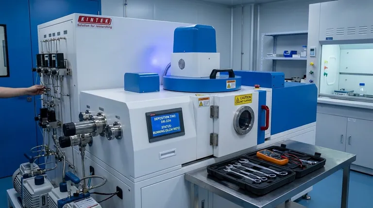
Sputtering systems are sophisticated and expensive. They require a high-vacuum chamber, powerful and stable power supplies (DC or RF), precise gas flow control systems for the sputtering gas (like Argon), and often, advanced substrate holders with heating or cooling capabilities. This capital outlay can be prohibitive for smaller labs or cost-sensitive production lines.
Operational Complexity
Operating a sputtering system effectively requires significant expertise. An operator must understand the complex interplay between gas pressure, power, target material, and chamber geometry to achieve the desired film properties. Furthermore, sputtering insulating materials requires a more complex and costly radio-frequency (RF) power supply instead of a simpler DC source, adding another layer of expense and operational difficulty.
Understanding the Trade-offs: Quality and Material Integrity
While known for producing dense, high-adhesion films, the sputtering process itself can introduce imperfections and limitations that must be carefully managed.
Risk of Film Contamination
Sputtering typically operates at a higher working pressure (a lower vacuum) than techniques like thermal evaporation. The chamber contains a significant amount of sputtering gas (e.g., Argon).
This environment increases the likelihood that stray atoms—from the sputtering gas itself or from residual gases like oxygen and water vapor in the chamber—will become embedded in the growing film. This incorporation of impurities can alter the film's electrical, optical, or mechanical properties.
Potential for Material Damage
The high-energy ionic bombardment is indiscriminate. It can damage delicate materials that are being deposited, such as organic solids or complex polymers. The kinetic energy can break chemical bonds, altering the material's fundamental structure and rendering it useless for its intended application.
Non-Uniformity Over Large Areas
For large-scale applications, such as coating architectural glass or large displays, achieving a perfectly uniform film can be challenging. In large rectangular sputtering systems, the plasma density can be uneven across the face of the target. This leads to different sputtering rates at different locations, resulting in variations in film thickness and properties across the substrate.
Making the Right Choice for Your Goal
Understanding these limitations is the first step in deciding if sputtering is the appropriate technology for your specific needs.
- If your primary focus is rapid deposition of simple metals with high purity: Thermal evaporation may be a faster and more cost-effective solution, as it operates in a higher vacuum with lower risk of gas incorporation.
- If you need to deposit complex alloys, refractory materials, or insulators with precise control: Sputtering is often the superior choice, but you must be prepared to manage its limitations regarding speed, cost, and potential substrate heating.
- If you are working with heat-sensitive or delicate substrates like polymers: The potential for ion-induced heat and radiation damage is a critical factor, and you may need to explore gentler deposition techniques or specialized low-energy sputtering processes.
Ultimately, choosing the right deposition method requires a clear understanding of the trade-offs between the quality you need and the practical constraints you face.
Summary Table:
| Limitation | Impact on Process |
|---|---|
| Low Deposition Rate | Slow film growth; unsuitable for high-throughput applications. |
| High Equipment Cost | Significant capital investment for vacuum chambers and power supplies. |
| Substrate Heating | Risk of damaging temperature-sensitive materials. |
| Film Contamination | Higher risk of gas impurities being embedded in the film. |
| Operational Complexity | Requires expert knowledge to manage parameters effectively. |
Need a Thin Film Solution Tailored to Your Specific Requirements?
While sputtering has its limitations, choosing the right equipment is crucial for success. KINTEK specializes in high-quality lab equipment and consumables, providing solutions that balance performance with practical constraints. Whether you are depositing complex alloys or working with delicate substrates, our expertise can help you optimize your process.
Contact our experts today to discuss how we can support your laboratory's unique needs and help you achieve superior results.
Visual Guide
Related Products
- Three-dimensional electromagnetic sieving instrument
- Chemical Vapor Deposition CVD Equipment System Chamber Slide PECVD Tube Furnace with Liquid Gasifier PECVD Machine
- Customer Made Versatile CVD Tube Furnace Chemical Vapor Deposition Chamber System Equipment
- Twin Screw Extruder Plastic Granulation Machine
- HFCVD Machine System Equipment for Drawing Die Nano-Diamond Coating
People Also Ask
- What type of materials can be separated using the method of sieving? A Guide to Efficient Particle Size Separation
- What are the precautions for sieving method? Ensure Accurate Particle Size Analysis
- What are the limitations of sieving? Understanding the Constraints of Particle Size Analysis
- Why is sieving equipment necessary for processing powder prior to hot extrusion of PEO? Ensure Cathode Film Uniformity
- What is sieving and how does it work? A Guide to Accurate Particle Size Analysis