Knowledge What is the maximum thickness of sputtering? Overcoming Stress and Adhesion Limits
Author avatar

Tech Team · Kintek Solution

Updated 4 days ago

What is the maximum thickness of sputtering? Overcoming Stress and Adhesion Limits

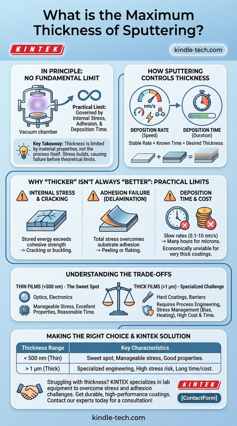
In principle, there is no fundamental upper limit to the thickness of a film you can create with sputtering. However, the practical maximum thickness is governed by internal film stress, adhesion, and deposition time, typically ranging from a few hundred nanometers to several microns for specialized applications.

The key takeaway is that sputtering thickness is not limited by the process itself, but by the material properties of the film being deposited. As thickness increases, internal stress builds, which can cause the film to crack, peel, or delaminate long before a theoretical limit is reached.

How Sputtering Controls Film Thickness

Sputtering is fundamentally a time-based process. You achieve a desired thickness by controlling how long you run the deposition at a known, stable rate.

The Role of Deposition Rate

The deposition rate is the speed at which the material accumulates on your substrate, often measured in angstroms or nanometers per second. This rate is determined by factors like the sputtering power, gas pressure, and the specific material being sputtered.

The Importance of Deposition Time

Once a stable deposition rate is established, film thickness becomes a direct function of time. To create a 50 nm film, you simply run the process for the required duration at a known rate. To create a thicker film, you run it for longer.

Why "Thicker" Isn't Always "Better": Practical Limitations

While you can theoretically run the process indefinitely, you will encounter practical failures long before you deposit a truly "thick" coating (e.g., millimeters). The most significant barrier is internal stress.

Internal Stress and Film Cracking

Nearly all sputtered films have some level of internal stress, which can be either compressive (pushing against itself) or tensile (pulling itself apart). This stress accumulates as the film gets thicker.

At a critical thickness, this stored energy becomes too great. The stress will exceed the film's own cohesive strength, causing it to crack or buckle to relieve the energy.

Adhesion Failure (Delamination)

Similarly, the total stress in the film can overcome its adhesion to the substrate. The thicker the film, the greater the total force pulling it away from the surface.

This results in delamination, where the film peels or flakes off entirely. This is one of the most common failure modes for thick sputtered films.

Deposition Time and Cost

Sputtering deposition rates are often quite slow, typically in the range of 0.1 to 10 nanometers per second.

Depositing a film that is several microns (thousands of nanometers) thick can take many hours. This makes the process extremely slow and economically unviable for applications where very thick coatings are needed quickly.

Understanding the Trade-offs

The "ideal" thickness is a balance between the desired physical property (like wear resistance) and the inherent limitations of stress and time.

Thin Films (< 500 nm): The Sweet Spot

This range, which includes the often-recommended 200 nm mark, is the sweet spot for many applications in optics and electronics.

In this regime, total stress is typically manageable, film properties are excellent, and deposition times are reasonable. The film is thick enough to perform its function without being so thick that it self-destructs.

Thick Films (> 1 µm): The Specialized Challenge

Achieving well-adhered, low-stress films thicker than one micron is possible but requires significant process engineering.

This often involves carefully tuning gas pressure, using substrate biasing, or incorporating periodic heat treatments to manage stress. These films are reserved for demanding applications like hard coatings for tools or thick corrosion barriers.

Making the Right Choice for Your Goal

Your target thickness should be dictated by your end goal and an understanding of the material's limitations.

  • If your primary focus is optical or electronic performance: Target the thinnest film that meets your performance specification, as this will minimize stress and cost.
  • If your primary focus is wear resistance or barrier protection: Thicker films are likely necessary, but you must plan for process development to manage stress and ensure strong adhesion.
  • If your primary focus is cost and throughput: Recognize that sputtering is not efficient for very thick films (many microns); evaluate if other methods like electroplating or thermal spray are a better fit.

Ultimately, the right thickness is determined not by the limits of the sputtering machine, but by the physical demands of your specific application.

Summary Table:

Thickness Range Key Characteristics & Considerations
< 500 nm (Thin Films) - Sweet spot for most applications (optics, electronics)
- Manageable stress levels
- Excellent film properties
- Reasonable deposition times
> 1 µm (Thick Films) - Requires specialized process engineering
- High risk of cracking/delamination
- Needs stress management techniques (bias, heating)
- Long deposition times, higher cost

Struggling to achieve the right sputtered film thickness for your application?

At KINTEK, we specialize in lab equipment and consumables that help you overcome the challenges of internal stress and adhesion. Our expertise ensures you get durable, high-performance coatings tailored to your specific needs—whether for thin-film electronics or thick protective barriers.

Let's optimize your deposition process together. Contact our experts today for a consultation!

Related Products

People Also Ask

Related Products

RF PECVD System Radio Frequency Plasma-Enhanced Chemical Vapor Deposition RF PECVD

RF PECVD System Radio Frequency Plasma-Enhanced Chemical Vapor Deposition RF PECVD

RF-PECVD is an acronym for "Radio Frequency Plasma-Enhanced Chemical Vapor Deposition." It deposits DLC (Diamond-like carbon film) on germanium and silicon substrates. It is utilized in the 3-12um infrared wavelength range.

Evaporation Boat for Organic Matter

Evaporation Boat for Organic Matter

The evaporation boat for organic matter is an important tool for precise and uniform heating during the deposition of organic materials.

Chemical Vapor Deposition CVD Equipment System Chamber Slide PECVD Tube Furnace with Liquid Gasifier PECVD Machine

Chemical Vapor Deposition CVD Equipment System Chamber Slide PECVD Tube Furnace with Liquid Gasifier PECVD Machine

KT-PE12 Slide PECVD System: Wide power range, programmable temp control, fast heating/cooling with sliding system, MFC mass flow control & vacuum pump.

Electron Beam Evaporation Coating Oxygen-Free Copper Crucible and Evaporation Boat

Electron Beam Evaporation Coating Oxygen-Free Copper Crucible and Evaporation Boat

Electron Beam Evaporation Coating Oxygen-Free Copper Crucible enables precise co-deposition of various materials. Its controlled temperature and water-cooled design ensure pure and efficient thin film deposition.

Aluminized Ceramic Evaporation Boat for Thin Film Deposition

Aluminized Ceramic Evaporation Boat for Thin Film Deposition

Vessel for depositing thin films; has an aluminum-coated ceramic body for improved thermal efficiency and chemical resistance. making it suitable for various applications.

VHP Sterilization Equipment Hydrogen Peroxide H2O2 Space Sterilizer

VHP Sterilization Equipment Hydrogen Peroxide H2O2 Space Sterilizer

A hydrogen peroxide space sterilizer is a device that uses vaporized hydrogen peroxide to decontaminate enclosed spaces. It kills microorganisms by damaging their cellular components and genetic material.

Cylindrical Resonator MPCVD Machine System Reactor for Microwave Plasma Chemical Vapor Deposition and Lab Diamond Growth

Cylindrical Resonator MPCVD Machine System Reactor for Microwave Plasma Chemical Vapor Deposition and Lab Diamond Growth

Learn about Cylindrical Resonator MPCVD Machine, the microwave plasma chemical vapor deposition method used for growing diamond gemstones and films in the jewelry and semi-conductor industries. Discover its cost-effective advantages over traditional HPHT methods.

Ceramic Evaporation Boat Set Alumina Crucible for Laboratory Use

Ceramic Evaporation Boat Set Alumina Crucible for Laboratory Use

It can be used for vapor deposition of various metals and alloys. Most metals can be evaporated completely without loss. Evaporation baskets are reusable.1

Ball Press Mold for Lab

Ball Press Mold for Lab

Explore versatile Hydraulic Hot Press molds for precise compression molding. Ideal for creating various shapes and sizes with uniform stability.

Electrolytic Electrochemical Cell for Coating Evaluation

Electrolytic Electrochemical Cell for Coating Evaluation

Looking for corrosion-resistant coating evaluation electrolytic cells for electrochemical experiments? Our cells boast complete specifications, good sealing, high-quality materials, safety, and durability. Plus, they're easily customizable to meet your needs.

Platinum Auxiliary Electrode for Laboratory Use

Platinum Auxiliary Electrode for Laboratory Use

Optimize your electrochemical experiments with our Platinum Auxiliary Electrode. Our high-quality, customizable models are safe and durable. Upgrade today!

Customizable High Pressure Reactors for Advanced Scientific and Industrial Applications

Customizable High Pressure Reactors for Advanced Scientific and Industrial Applications

This laboratory-scale high-pressure reactor is a high-performance autoclave engineered for precision and safety in demanding research and development environments.

Laboratory Vibratory Sieve Shaker Machine Slap Vibrating Sieve

Laboratory Vibratory Sieve Shaker Machine Slap Vibrating Sieve

KT-T200TAP is a slapping and oscillating sieving instrument for laboratory desktop use, with 300 rpm horizontal circular motion and 300 vertical slapping motions to simulate manual sieving to help sample particles pass through better.

Non Consumable Vacuum Arc Induction Melting Furnace

Non Consumable Vacuum Arc Induction Melting Furnace

Explore the benefits of Non-Consumable Vacuum Arc Furnace with high melting point electrodes. Small, easy to operate & eco-friendly. Ideal for laboratory research on refractory metals & carbides.

High Performance Laboratory Freeze Dryer

High Performance Laboratory Freeze Dryer

Advanced lab freeze dryer for lyophilization, preserving biological & chemical samples efficiently. Ideal for biopharma, food, and research.

Circulating Water Vacuum Pump for Laboratory and Industrial Use

Circulating Water Vacuum Pump for Laboratory and Industrial Use

Efficient circulating water vacuum pump for labs - oil-free, corrosion-resistant, quiet operation. Multiple models available. Get yours now!

Platinum Sheet Electrode for Laboratory and Industrial Applications

Platinum Sheet Electrode for Laboratory and Industrial Applications

Elevate your experiments with our Platinum Sheet Electrode. Crafted with quality materials, our safe and durable models can be tailored to fit your needs.

Electron Beam Evaporation Coating Conductive Boron Nitride Crucible BN Crucible

Electron Beam Evaporation Coating Conductive Boron Nitride Crucible BN Crucible

High-purity and smooth conductive boron nitride crucible for electron beam evaporation coating, with high temperature and thermal cycling performance.

Desktop Fast High Pressure Laboratory Autoclave Sterilizer 16L 24L for Lab Use

Desktop Fast High Pressure Laboratory Autoclave Sterilizer 16L 24L for Lab Use

The desktop fast steam sterilizer is a compact and reliable device used for rapid sterilization of medical, pharmaceutical, and research items.

Polygon Press Mold for Lab

Polygon Press Mold for Lab

Discover precision polygon press molds for sintering. Ideal for pentagon-shaped parts, our molds ensure uniform pressure and stability. Perfect for repeatable, high-quality production.


Leave Your Message