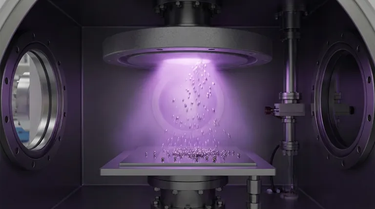
At its core, sputtering is a physical process of atomic-scale erosion. It uses high-energy particles in a plasma to physically knock atoms off the surface of a solid material, called a target. These ejected atoms then travel through a vacuum and deposit onto another surface, known as a substrate, where they accumulate to form an exceptionally thin and uniform film.
Sputtering is not a chemical reaction but a momentum transfer event. The process is fundamentally about controlling a collision cascade within a vacuum, allowing for the precise construction of thin films atom-by-atom for use in advanced electronics, optics, and nanotechnology.
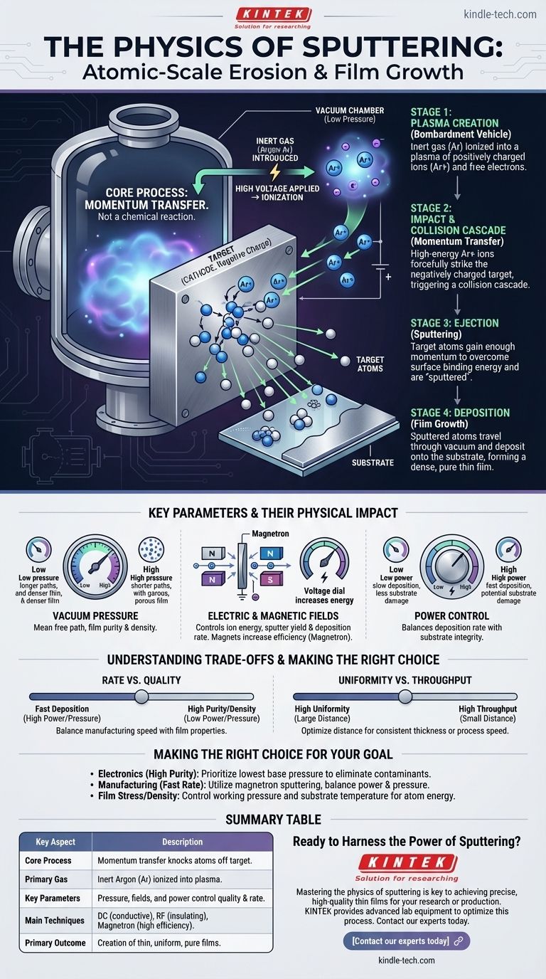
The Core Physics: A Collision Cascade
The entire sputtering process is a carefully orchestrated sequence of physical events. It begins with the creation of a plasma and ends with the formation of a new material layer.
Creating the Bombardment Vehicle: The Plasma
First, a vacuum chamber is evacuated to a very low pressure to remove contaminants like oxygen and water vapor, which would otherwise corrupt the film.
An inert gas, most commonly Argon (Ar), is then introduced into the chamber, raising the pressure slightly. A high voltage is applied, creating a strong electric field that strips electrons from the Argon atoms.
This process, called ionization, creates a plasma—a superheated gas consisting of positively charged Argon ions (Ar+) and free electrons.
The Impact: Momentum Transfer
The target material, which will become the thin film, is given a strong negative electrical charge, making it a cathode. The positively charged Argon ions are forcefully accelerated by the electric field and slam into this negatively charged target.
When a high-energy ion strikes the target, it triggers a collision cascade. It transfers its momentum to the atoms it hits, which in turn hit other atoms, creating a chain reaction of collisions just below the target's surface.
The Ejection: Overcoming Binding Energy
Atoms near the surface that receive sufficient momentum from this cascade can overcome the forces holding them to the target (their surface binding energy).
These atoms are physically ejected, or "sputtered," from the target. They travel away from the target in a "line-of-sight" trajectory through the low-pressure environment.
The Deposition: Film Growth
These ejected target atoms eventually strike the substrate (e.g., a silicon wafer, glass panel, or plastic part) that has been strategically placed in the chamber.
Upon arrival, the atoms condense on the substrate's surface. They nucleate into small islands, which then grow and coalesce to form a continuous, dense, and highly pure thin film.
Key Parameters and Their Physical Impact
The quality, deposition rate, and characteristics of the sputtered film are not accidental. They are directly controlled by manipulating the physics of the process.
The Role of Vacuum Pressure
The initial base pressure (high vacuum) is critical for film purity. The subsequent working pressure of the inert gas determines the "mean free path"—the average distance a sputtered atom can travel before hitting a gas ion.
Lower pressure means a longer mean free path, resulting in more energetic atoms hitting the substrate and creating a denser film. Higher pressure can increase deposition speed but may lead to more porous films due to energy loss from collisions.
The Power of Electric and Magnetic Fields
The applied voltage directly controls the energy of the bombarding ions. Higher voltage leads to more energetic collisions and a higher "sputter yield" (more atoms ejected per ion), increasing the deposition rate.
In modern systems, magnets are placed behind the target (magnetron sputtering). This magnetic field traps electrons near the target surface, dramatically increasing the efficiency of Argon ionization. This allows the process to run at lower pressures and achieve much higher deposition rates.
Understanding the Trade-offs
Sputtering is a powerful technique, but its application requires balancing competing factors. Understanding these trade-offs is key to successful implementation.
Rate vs. Quality
Achieving a high deposition rate is often a primary industrial goal. This can be accomplished by increasing power or pressure. However, excessively high power can damage the substrate, while high pressure can lead to gas atoms becoming trapped in the film, reducing its purity and density.
Uniformity vs. Throughput
Placing the substrate very close to the target will increase the deposition rate but may result in a non-uniform film thickness across the substrate surface. Increasing the target-to-substrate distance improves uniformity but at the cost of a slower process and wasted target material.
Simplicity vs. Control
Basic DC sputtering is simple but only works for conductive targets. To deposit insulating materials (ceramics, oxides), a more complex technique called RF (Radio Frequency) sputtering is required, which uses an alternating electric field to prevent charge buildup on the target.
Making the Right Choice for Your Goal
The physics you choose to prioritize depends entirely on the desired outcome for your thin film.
- If your primary focus is a high-purity film for electronics: Prioritize achieving the lowest possible base pressure to eliminate contaminants before beginning deposition.
- If your primary focus is a fast deposition rate for manufacturing: Utilize magnetron sputtering and carefully balance power and working gas pressure to maximize throughput without sacrificing essential film quality.
- If your primary focus is controlling film stress or density: Pay close attention to the working pressure and substrate temperature, as these directly influence the energy of atoms as they arrive at the substrate.
By mastering the interplay of plasma, pressure, and electromagnetism, you transform this fundamental physical process into a precise tool for advanced material fabrication.
Summary Table:
| Key Aspect | Description |
|---|---|
| Core Process | Momentum transfer from high-energy ions knocks atoms off a target material. |
| Primary Gas | Inert gas (e.g., Argon) is ionized to create the bombarding plasma. |
| Key Parameters | Vacuum pressure, electric/magnetic fields, and power control film quality and rate. |
| Main Techniques | DC Sputtering (conductive targets), RF Sputtering (insulating targets), Magnetron Sputtering (high efficiency). |
| Primary Outcome | Creation of exceptionally thin, uniform, and pure films on a substrate. |
Ready to Harness the Power of Sputtering in Your Lab?
Mastering the physics of sputtering is key to achieving precise, high-quality thin films for your research or production. KINTEK specializes in providing the advanced lab equipment and consumables you need to optimize this process, from robust vacuum systems to high-purity targets.
Contact our experts today to discuss your specific application—whether it's for advanced electronics, optics, or nanotechnology—and discover how our solutions can enhance your deposition rate, improve film uniformity, and ensure the purity critical to your success.
Visual Guide
Related Products
- Spark Plasma Sintering Furnace SPS Furnace
- Vacuum Induction Melting Spinning System Arc Melting Furnace
- Chemical Vapor Deposition CVD Equipment System Chamber Slide PECVD Tube Furnace with Liquid Gasifier PECVD Machine
- Customer Made Versatile CVD Tube Furnace Chemical Vapor Deposition Chamber System Equipment
People Also Ask
- What is the pressure for spark plasma sintering? A Guide to Optimizing SPS Parameters
- What is the mechanism of SPS process? A Deep Dive into Rapid, Low-Temperature Sintering
- What is SPS sintering method? A Guide to High-Speed, High-Performance Material Fabrication
- Why are Spark Plasma Sintering (SPS) furnaces or hot presses utilized in the preparation of Li3PS4 solid electrolytes?
- What is the theory of spark plasma sintering? A Guide to Rapid, Low-Temperature Densification


