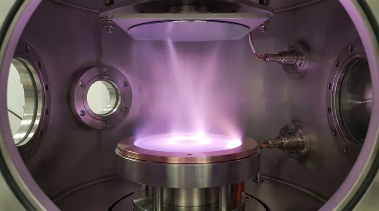
At its core, the sputter target process is a physical vapor deposition (PVD) method used to create exceptionally thin films of material. In a high-vacuum chamber, a high-voltage electrical field accelerates ions from an inert gas (like argon) into a source material, known as the target. This high-energy bombardment physically knocks atoms off the target, which then travel through the vacuum and deposit onto a substrate, building the desired thin film one atom at a time.
The central principle of sputtering is the transfer of momentum. It uses energetic gas ions as microscopic projectiles to physically eject atoms from a source material, which then condense onto a surface to form a uniform coating.
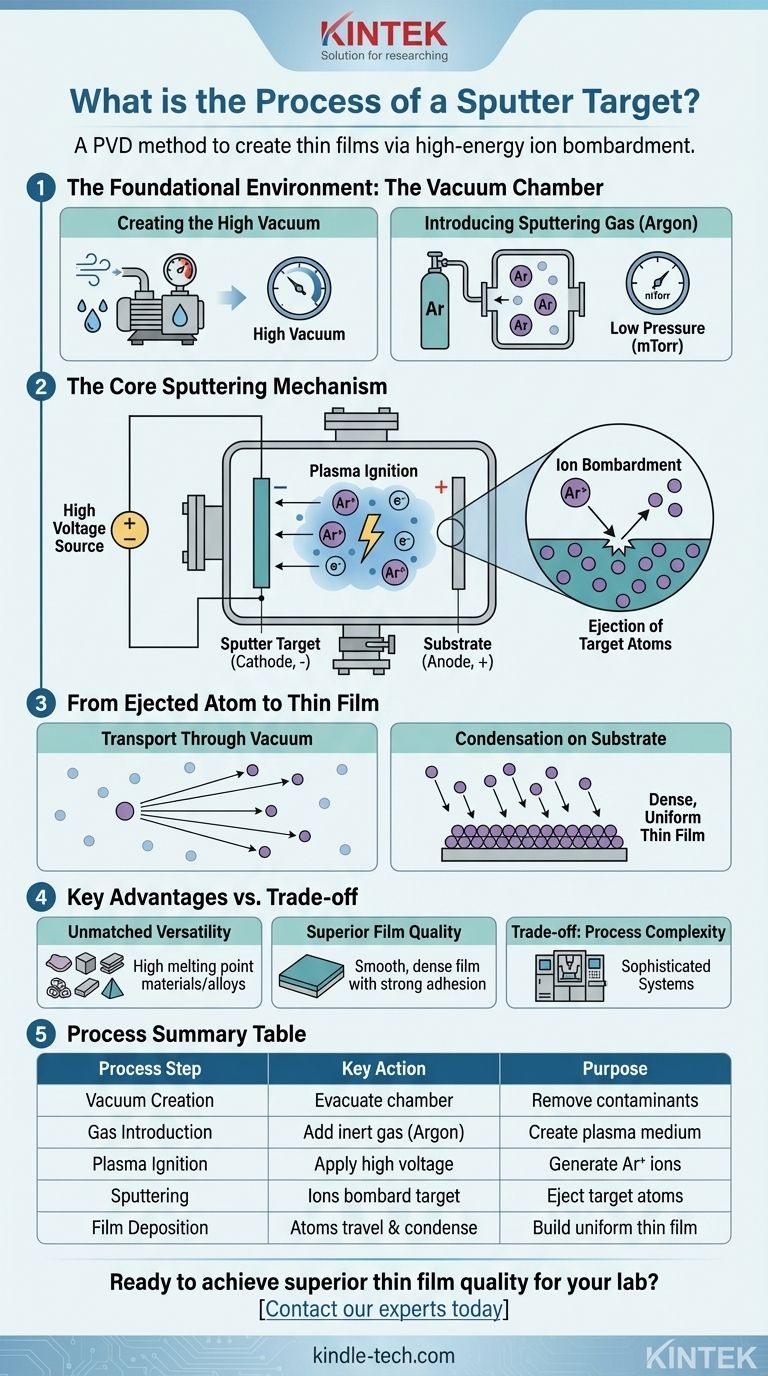
The Foundational Environment: The Vacuum Chamber
To understand the sputtering process, we must first look at the highly controlled environment where it occurs. The quality of the final film is entirely dependent on the purity of this environment.
Creating the High Vacuum
The process begins by placing the target material and the substrate into a sealed chamber. This chamber is then evacuated to a very high vacuum, removing air, water vapor, and other background gases.
This initial step is critical to prevent contamination. Any unwanted molecules would interfere with the process and become embedded in the thin film, compromising its purity and performance.
Introducing the Sputtering Gas
Once a high vacuum is achieved, a small, precisely controlled amount of an inert gas is introduced. Argon (Ar) is the most common choice because it is chemically inert, relatively heavy, and cost-effective.
The chamber pressure is stabilized at a very low level, typically in the milliTorr range. This low pressure ensures there are enough gas atoms to create a plasma but not so many that they obstruct the path of the sputtered atoms traveling to the substrate.
The Core Sputtering Mechanism
With the environment set, the active part of the process can begin. This is a sequence of events driven by plasma physics and electromagnetism.
Igniting the Plasma
A high voltage is applied within the chamber, creating a strong electric field. This energy strips electrons from the argon atoms, creating a mixture of free electrons and positively charged argon ions (Ar+). This energized, ionized gas is known as a plasma or gaseous discharge.
The Role of the Target (Cathode)
The source material to be deposited, the sputter target, is configured to act as the cathode, giving it a strong negative electrical charge. The substrate, where the film will be formed, typically serves as the anode.
Ion Acceleration and Bombardment
The positively charged argon ions (Ar+) in the plasma are now strongly attracted to the negatively charged target. The electric field accelerates these ions, causing them to slam into the surface of the target with significant kinetic energy.
Ejection of Target Atoms
This high-energy ion bombardment is the "sputtering" event. The impact's energy is transferred to the atoms of the target material, knocking them loose and ejecting them from the surface. This is a purely physical ejection, not a chemical or thermal (melting) process.
From Ejected Atom to Thin Film
The final stage of the process involves the transport and deposition of the material that has been liberated from the target.
Transport Through the Vacuum
The ejected, neutral atoms from the target travel through the low-pressure chamber. Because the pressure is so low, they can travel in a relatively straight line from the target toward the substrate with minimal collisions with argon gas atoms.
Condensation on the Substrate
When these atoms arrive at the substrate, they condense on its surface. Over time, millions of these arriving atoms build up layer by layer, forming a dense, uniform, and highly pure thin film.
Understanding the Key Advantages
Sputtering is not the only method for creating thin films, but it possesses unique strengths that make it indispensable in many advanced industries.
Unmatched Material Versatility
Because sputtering is a physical process, it does not rely on melting or evaporating the source material. This makes it exceptionally effective for depositing materials with very high melting points, such as refractory metals, or for creating films of complex alloys whose compositions would change if melted.
Superior Film Quality
The sputtered atoms arrive at the substrate with higher kinetic energy compared to atoms in a thermal evaporation process. This typically results in films that are denser, more uniform, and have stronger adhesion to the substrate.
The Trade-off: Process Complexity
The primary trade-off is the complexity and cost of the equipment. Achieving and maintaining the required high vacuum and generating a stable plasma demands sophisticated and expensive systems compared to simpler deposition methods.
Making the Right Choice for Your Application
Understanding this process allows you to determine where it fits best.
- If your primary focus is material versatility: Sputtering is the superior choice for depositing refractory metals, ceramics, or complex alloys that cannot be handled by thermal evaporation.
- If your primary focus is film quality and adhesion: The high energy of the sputtering process produces dense, durable, and well-adhered films ideal for optics, semiconductors, and protective coatings.
- If your primary focus is precise composition control: Sputtering faithfully transfers the composition of the target to the substrate, making it essential for applications requiring specific alloy or compound stoichiometry.
Ultimately, sputtering provides a powerful and precise tool for engineering materials at the atomic scale.
Summary Table:
| Process Step | Key Action | Purpose |
|---|---|---|
| Vacuum Creation | Evacuate chamber | Remove contaminants for high-purity films |
| Gas Introduction | Add inert gas (Argon) | Create plasma medium for ion bombardment |
| Plasma Ignition | Apply high voltage | Generate Ar+ ions to accelerate toward target |
| Sputtering | Ions bombard target | Eject target atoms via momentum transfer |
| Film Deposition | Atoms travel & condense | Build uniform, dense thin film on substrate |
Ready to achieve superior thin film quality for your lab? The sputtering process is key for high-performance applications in semiconductors, optics, and protective coatings. KINTEK specializes in high-purity sputter targets and lab equipment to ensure your deposition processes are precise and reliable. Contact our experts today to discuss how our solutions can enhance your research and production outcomes.
Visual Guide
Related Products
- Multifunctional Electrolytic Electrochemical Cell Water Bath Single Layer Double Layer
- Reference Electrode Calomel Silver Chloride Mercury Sulfate for Laboratory Use
- Laboratory CVD Boron Doped Diamond Materials
- Square Lab Press Mold for Laboratory Applications
- Electron Beam Evaporation Coating Oxygen-Free Copper Crucible and Evaporation Boat
People Also Ask
- What are the procedures for after using a double-layer water-bath electrolytic cell? Ensure Equipment Longevity and Data Accuracy
- What is the typical experimental system used with a double-layer water-bath electrolytic cell? Achieve Precise Electrochemical Control
- What is the typical volume range of the multifunctional electrolytic cell? Choosing the Right Size for Your Lab
- How can water and gas leaks be prevented in a double-layer water-bath electrolytic cell? A Guide to Proactive Maintenance
- What steps should be taken before using a double-layer water-bath electrolytic cell? Ensure Accurate Electrochemical Results


