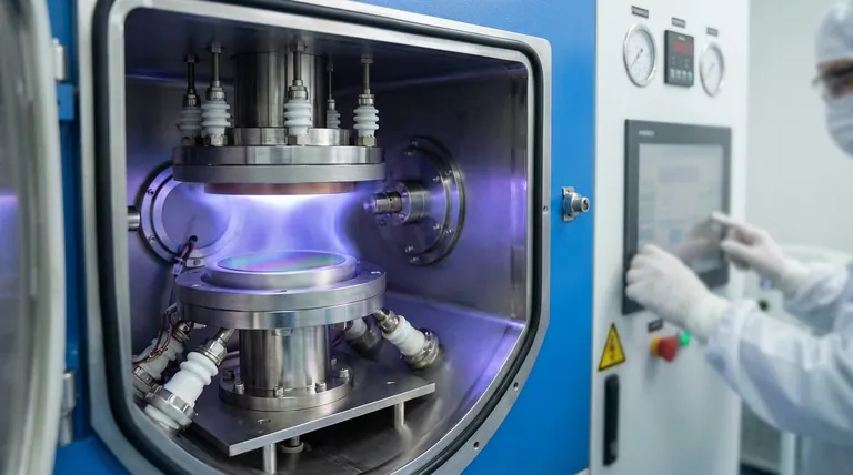
In essence, sputtering is a highly controlled vacuum deposition process used to apply an exceptionally thin and uniform layer of material onto a surface. Its primary purpose is to create high-performance coatings, known as thin films, with excellent purity, density, and adhesion for a vast range of industrial and scientific applications, from computer chips to optical lenses.
The core challenge in advanced manufacturing is often creating a flawless, atom-thin coating on a surface. Sputtering solves this not by melting or chemical reaction, but by using a physical process—energetic ion bombardment—to precisely transfer material from a source to a substrate, offering unparalleled control and material versatility.
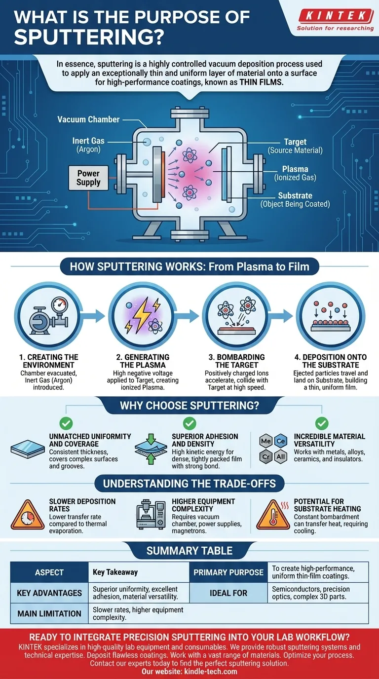
How Sputtering Works: From Plasma to Film
Sputtering is a form of Physical Vapor Deposition (PVD). The process takes place inside a sealed vacuum chamber and relies on a sequence of carefully controlled physical events.
Creating the Environment
First, the chamber is evacuated to a high vacuum to remove air and other contaminants. Then, a small, controlled amount of an inert process gas, most commonly argon, is introduced into the chamber.
Generating the Plasma
A high negative voltage is applied to the source material, known as the target. This electrical potential energizes the chamber, stripping electrons from the argon atoms and creating a plasma—a glowing, ionized gas containing positively charged argon ions.
Bombarding the Target
These positively charged ions are accelerated by the electric field, causing them to collide with the negatively charged target at high speed. Think of it as a form of atomic-scale sandblasting.
Deposition onto the Substrate
Each ion impact transfers enough energy to knock atoms or molecules loose from the target material. These ejected particles travel in a straight line through the vacuum and land on the object being coated, known as the substrate, gradually building up a thin, uniform film.
Why Choose Sputtering? The Key Advantages
Engineers and scientists choose sputtering when the quality and performance of the coating are critical. It offers several distinct advantages over other deposition methods.
Unmatched Uniformity and Coverage
Because the sputtered atoms emanate from the entire surface of a large target, the resulting film is exceptionally uniform in thickness. This allows for consistent coating of even complex, non-flat surfaces with features like grooves or steps.
Superior Adhesion and Density
The sputtered particles arrive at the substrate with significant kinetic energy. This energy helps them form a dense, tightly packed film with a very strong bond to the substrate surface, which prevents the coating from flaking or peeling.
Incredible Material Versatility
Unlike some processes that rely on melting, sputtering is a physical process that works with an enormous range of materials. It can deposit metals, alloys, ceramics, and other insulating materials with high purity, making it a cornerstone of modern electronics and optics.
Understanding the Trade-offs
While powerful, sputtering is not the universal solution for every coating need. Understanding its limitations is key to making an informed decision.
Slower Deposition Rates
Compared to thermal evaporation, where material is simply boiled off, sputtering is a slower, more deliberate process. The rate of material transfer is lower, which can increase process time and cost for very thick coatings.
Higher Equipment Complexity
A sputtering system requires a vacuum chamber, high-voltage power supplies, gas flow controllers, and often a magnetron to confine the plasma. This makes the initial equipment investment more significant than for simpler methods like electroplating.
Potential for Substrate Heating
The constant bombardment of energetic particles can transfer heat to the substrate. While not a melting process, this can be a concern when coating heat-sensitive materials like certain plastics or biological samples, requiring active cooling.
Making the Right Choice for Your Application
The decision to use sputtering is driven entirely by the final performance requirements of the coating.
- If your primary focus is precision and film quality: Sputtering is the superior choice for applications like semiconductor manufacturing, precision optics, and magnetic storage media where purity and uniformity are non-negotiable.
- If your primary focus is coating complex geometries: Sputtering excels at providing an even, consistent coating on parts with intricate shapes that are challenging for line-of-sight deposition methods.
- If your primary focus is depositing advanced materials: Sputtering is one of the few techniques capable of depositing high-performance ceramics, dielectrics, and other compounds that cannot be easily evaporated.
Ultimately, sputtering empowers the creation of advanced materials by providing atomic-level control over the structure and properties of a surface.
Summary Table:
| Aspect | Key Takeaway |
|---|---|
| Primary Purpose | To create high-performance, uniform thin-film coatings. |
| Key Advantages | Superior uniformity, excellent adhesion, and incredible material versatility (metals, alloys, ceramics). |
| Ideal For | Applications requiring precision, like semiconductors, precision optics, and complex 3D parts. |
| Main Limitation | Slower deposition rates and higher equipment complexity compared to some methods. |
Ready to Integrate Precision Sputtering into Your Lab Workflow?
Sputtering is the gold standard for creating high-performance thin films, but achieving consistent results requires reliable equipment and expert support. KINTEK specializes in high-quality lab equipment and consumables, serving the precise needs of laboratories in R&D, semiconductor manufacturing, and materials science.
We provide the robust sputtering systems and technical expertise to help you:
- Deposit flawless coatings with unmatched uniformity and adhesion.
- Work with a vast range of materials, from metals to advanced ceramics.
- Optimize your process for maximum efficiency and yield.
Let's discuss how our solutions can enhance your research and production. Contact our experts today to find the perfect sputtering solution for your specific application.
Visual Guide
Related Products
- Lab Sterile Slapping Type Homogenizer for Tissue Mashing and Dispersing
- Spark Plasma Sintering Furnace SPS Furnace
- Single Punch Manual Tablet Press Machine TDP Tablet Punching Machine
People Also Ask
- What is the primary function of an ultrasonic cleaner in coating? Achieve Unmatched Substrate Purity for PVD Adhesion
- How does a laboratory automatic masticator or homogenizer facilitate the processing of biofilm samples? Optimize Accuracy
- What is the role of an ultrasonic cleaner during magnesium alloy coating? Ensure Superior Adhesion and Surface Purity
- What role does an ultrasonic cleaner play in the pre-treatment of 4140 steel? Ensure Uniform Nitriding Activation
- How do lab stirrers & homogenizers ensure uniform distribution? Optimize Your Complex Multiphase Chemical Mixing


