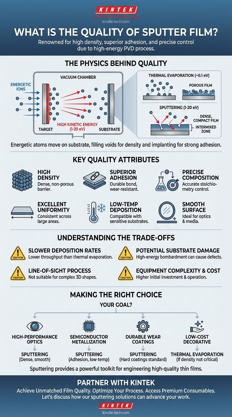
In short, films produced by sputtering are renowned for their exceptional quality, characterized by high density, superior adhesion to the substrate, and precise control over material composition. This quality stems directly from the energetic nature of the physical vapor deposition (PVD) process itself, where atoms arrive at the substrate with significantly more energy than in other methods like thermal evaporation.
The "quality" of a sputter film is not a single property, but a collection of desirable physical characteristics. Sputtering excels at producing dense, pure, and strongly-adhered films, making it a preferred method for demanding optical, electronic, and protective applications.
The Physics Behind Sputtering's Quality
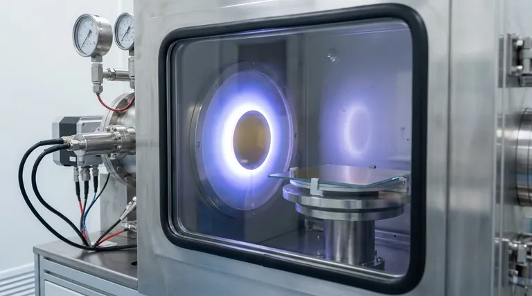
To understand the quality of a sputter film, you must first understand the process. Sputtering involves bombarding a source material, known as a target, with energetic ions in a vacuum. This bombardment ejects or "sputters" atoms from the target, which then travel and deposit onto a substrate, forming the thin film.
The Power of High Kinetic Energy
The key differentiator for sputtering is the high kinetic energy of the deposited atoms.
Atoms deposited via thermal evaporation arrive with very low energy (~0.1 eV). In contrast, sputtered atoms arrive with energies of several electron volts (1-20 eV), which is 10 to 100 times greater.
This additional energy is the primary reason for the superior film properties.
The Result: Dense, Compact Films
The energetic sputtered atoms do not simply "stick" where they land. They have enough energy to move around on the substrate surface for a short time.
This mobility allows them to find and fill in voids, resulting in a film that is significantly denser and less porous than an evaporated film. This density is critical for creating effective barrier layers against moisture or for producing stable optical coatings with a high refractive index.
Superior Adhesion
When high-energy sputtered atoms impact the substrate, they can physically implant into the first few atomic layers.
This creates an "intermixed zone" between the film and the substrate, forming an incredibly strong, durable bond. This superior adhesion is a hallmark of sputtering and is vital for coatings that must withstand mechanical stress or wear.
Key Quality Attributes of Sputter Films
The unique physics of the sputtering process translates into several measurable quality attributes that make it the process of choice for many high-performance applications.
Precise Compositional Control
Sputtering is an excellent method for depositing alloys or compound materials like oxides and nitrides.
Because the process physically ejects atoms from the target, the composition of the resulting film very closely matches the composition of the target. This allows for precise control over the film's stoichiometry, which is crucial for controlling its electrical, optical, and chemical properties.
Excellent Uniformity
Modern magnetron sputtering systems are engineered to deposit films with excellent thickness uniformity across large areas.
This capability is essential for manufacturing products like architectural glass, large-screen displays, and semiconductor wafers, where consistent performance across the entire surface is non-negotiable.
Low-Temperature Deposition
While the sputtered atoms are energetic, the overall process does not significantly heat the substrate.
This makes sputtering compatible with temperature-sensitive substrates like plastics or pre-processed semiconductor devices, a key advantage over high-temperature processes like chemical vapor deposition (CVD).
Smooth Surface Morphology
The same atomic mobility that creates dense films also promotes the growth of very smooth surfaces. Low surface roughness is critical for applications like mirrors, optical filters, and magnetic storage media where scattering or surface defects would degrade performance.
Understanding the Trade-offs
No deposition technique is perfect for every scenario. To make an informed decision, you must understand the limitations of sputtering.
Slower Deposition Rates
For many materials, especially simple metals like aluminum, sputtering has a lower deposition rate than thermal evaporation. This can impact manufacturing throughput and increase the cost per part in high-volume production.
Potential for Substrate Damage
The same high-energy bombardment that improves adhesion can also cause damage to the substrate. In highly sensitive applications, such as certain semiconductor devices, this can introduce defects into the crystal lattice, a phenomenon known as radiation damage.
Line-of-Sight Limitations
Sputtering is a line-of-sight process. It is not well-suited for uniformly coating complex, three-dimensional shapes with deep trenches or undercuts. Processes like atomic layer deposition (ALD) or CVD offer superior conformality for such geometries.
Equipment Complexity and Cost
Sputtering systems are sophisticated vacuum chambers requiring high-power electrical supplies, gas handling, and expensive target materials. This makes the initial capital investment and ongoing operational costs higher than for a simple thermal evaporator.
Making the Right Choice for Your Goal
The decision to use sputtering should be based on the specific performance requirements of your film.
- If your primary focus is high-performance optical coatings: Sputtering is an ideal choice due to the dense, smooth, and environmentally stable films it produces.
- If your primary focus is metallization for semiconductor devices: Sputtering provides the superior adhesion, purity, and low-temperature processing necessary for reliable interconnects and barrier layers.
- If your primary focus is durable, wear-resistant coatings: The exceptional adhesion and density of sputtered hard coatings (e.g., TiN) make it the industry standard.
- If your primary focus is low-cost, high-volume decorative coatings: Thermal evaporation may be a more cost-effective choice if the ultimate film density and adhesion are not critical.
Ultimately, sputtering provides a powerful toolkit for engineering high-quality thin films with specific, controllable, and repeatable properties.
Summary Table:
| Key Quality Attribute | Description | Benefit |
|---|---|---|
| High Density | Energetic atoms fill voids, creating dense, non-porous films. | Superior barrier properties, stable optical performance. |
| Superior Adhesion | High-energy impact creates a strong intermixed zone with the substrate. | Excellent durability and wear resistance. |
| Precise Composition | Film composition closely matches the target material. | Accurate control over electrical, optical, and chemical properties. |
| Excellent Uniformity | Consistent thickness across large areas like wafers or display glass. | Reliable, repeatable performance in manufacturing. |
| Smooth Surface | Atomic mobility promotes low surface roughness. | Ideal for optical coatings and magnetic media. |
| Low-Temperature Process | Does not significantly heat the substrate. | Compatible with temperature-sensitive materials like plastics. |
Ready to Engineer High-Quality Thin Films for Your Lab?
Sputtering is the gold standard for creating dense, adherent, and precisely controlled thin films for critical applications in optics, electronics, and materials science. KINTEK specializes in providing advanced sputtering equipment and consumables to meet the exacting demands of your laboratory.
Partner with KINTEK to:
- Achieve Unmatched Film Quality: Leverage our expertise to produce films with superior density, adhesion, and purity.
- Optimize Your Process: Our team can help you select the right sputtering system and targets for your specific research or production goals.
- Access Premium Consumables: Ensure consistent, high-quality results with our reliable sputtering targets and accessories.
Let's discuss how our sputtering solutions can advance your work. Contact our thin film experts today for a personalized consultation.
Visual Guide
Related Products
People Also Ask
- What is the thinnest coating? Unlocking Unique Properties at the Atomic Scale
- What is the difference between single layer film and multi layer film? A Guide to Material Selection
- What are the properties of Aluminium (Al) relevant to its use in coatings? High Reflectivity & Conductivity Explored
- What is organic thin film? A Guide to Engineered Molecular Layers for Advanced Tech
- Is there a way to test lithium batteries? Understand Voltage vs. True Health
