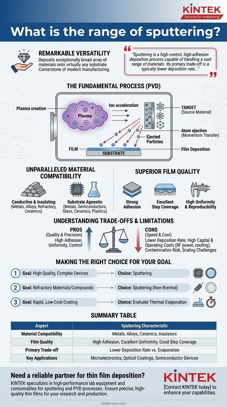
In practice, the "range" of sputtering refers to its remarkable versatility. The technique allows for the deposition of an exceptionally broad array of materials—including metals, alloys, ceramics, and even some plastics—onto virtually any substrate. This versatility, combined with the high quality of the resulting films, makes it a cornerstone of modern manufacturing for everything from microelectronics to optical coatings.
Sputtering is a high-control, high-adhesion deposition process capable of handling a vast range of materials. Its primary trade-off is a typically lower deposition rate compared to less precise methods like thermal evaporation.
What Defines Sputtering's Versatility?
To understand sputtering's wide-ranging capabilities, you must first understand its fundamental mechanism. Unlike processes that melt materials, sputtering is a physical momentum-transfer process.
The Fundamental Process
Sputtering is a form of Physical Vapor Deposition (PVD). It begins by creating a plasma inside a vacuum chamber. Ions from this plasma are accelerated into a source material, known as the target.
The impact of these high-energy ions knocks atoms or molecules loose from the target. These ejected particles travel in a straight line and deposit onto a nearby surface, called the substrate, forming a thin, highly uniform film.
Unparalleled Material Compatibility
Because sputtering does not rely on melting the source material, it can be used with an enormous variety of substances.
The process can effectively deposit conductive or insulating materials, including pure metals, complex alloys, and refractory materials with extremely high melting points. It is also a primary method for depositing ceramic compounds like oxides and nitrides.
Furthermore, the substrate material is not a limiting factor. Films can be deposited on metals, semiconductors, glass, ceramics, and plastics with excellent results.
Superior Film Quality
The energy of the sputtered atoms leads to films with desirable physical properties that are often difficult to achieve with other methods.
Key characteristics include strong adhesion to the substrate and excellent step coverage, meaning the film conforms evenly over non-flat or textured surfaces. The process allows for very precise control over deposition time and power, resulting in excellent film thickness uniformity and high reproducibility from one run to the next.
Understanding the Trade-offs and Limitations
No technique is without its compromises. While sputtering is highly capable, its operational characteristics present clear trade-offs.
Deposition Rate vs. Quality
The most significant trade-off is speed. Sputtering generally has a lower deposition rate than other PVD methods like thermal evaporation. The process of ejecting atoms one by one is inherently slower than boiling material from a molten source.
Equipment and Operating Costs
Sputtering systems require a significant capital investment. The need for robust vacuum chambers, high-voltage power supplies, and often a cooling system to manage heat from the plasma increases both initial cost and energy consumption.
For depositing insulating materials, a more complex RF (Radio Frequency) power supply is required instead of a simpler DC source, which further adds to the cost.
Potential for Contamination
The quality of the sputtered film depends on the purity of both the target material and the vacuum environment. Impurities in the target can be transferred to the film, and any residual gas in the chamber can become incorporated as well.
Scaling Challenges
While uniformity is excellent on a small scale, maintaining a perfectly even plasma density over very large rectangular targets (e.g., >1 meter) can be challenging. This can lead to slight variations in film thickness across large substrates, requiring careful system design to mitigate.
Making the Right Choice for Your Goal
Selecting the correct deposition method requires aligning the technique's strengths with your project's primary objective. Sputtering's value lies in its precision, quality, and material flexibility.
- If your primary focus is high-quality, uniform films for complex devices: Sputtering is the superior choice due to its precise control over thickness, composition, and strong film adhesion.
- If your primary focus is depositing refractory metals, alloys, or compounds: Sputtering's non-thermal nature makes it ideal for materials that are difficult or impossible to deposit via evaporation.
- If your primary focus is rapid, low-cost coating of simple materials: You should evaluate thermal evaporation as a potentially faster and more economical alternative.
Ultimately, understanding the trade-offs between sputtering's quality and versatility versus its speed and cost is the key to making an informed decision.
Summary Table:
| Aspect | Sputtering Characteristic |
|---|---|
| Material Compatibility | Metals, Alloys, Ceramics, Insulators |
| Film Quality | High Adhesion, Excellent Uniformity, Good Step Coverage |
| Primary Trade-off | Lower Deposition Rate vs. Evaporation |
| Key Applications | Microelectronics, Optical Coatings, Semiconductor Devices |
Need a reliable partner for your thin film deposition?
KINTEK specializes in high-performance lab equipment and consumables for sputtering and other PVD processes. Whether you are developing next-generation microchips, durable optical coatings, or advanced semiconductor devices, our expertise and products ensure you achieve the precise, high-quality thin films your research and production demand.
Contact KINTEK today to discuss how our solutions can enhance your laboratory's capabilities and drive your projects forward.
Visual Guide
Related Products
- Spark Plasma Sintering Furnace SPS Furnace
- Vacuum Induction Melting Spinning System Arc Melting Furnace
- Chemical Vapor Deposition CVD Equipment System Chamber Slide PECVD Tube Furnace with Liquid Gasifier PECVD Machine
- Customer Made Versatile CVD Tube Furnace Chemical Vapor Deposition Chamber System Equipment
People Also Ask
- What is the mechanism of SPS process? A Deep Dive into Rapid, Low-Temperature Sintering
- What technical advantages does a Spark Plasma Sintering (SPS) furnace offer for LZP ceramics? Enhance Ionic Conductivity
- What is the process fundamentals of spark plasma sintering? Achieve Rapid, High-Density Material Consolidation
- What is the pressure for spark plasma sintering? A Guide to Optimizing SPS Parameters
- What is the difference between spark plasma sintering and flash sintering? A Guide to Advanced Sintering Methods


