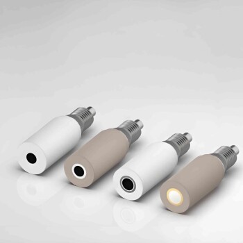
In the simplest terms, a "used sputtering target" is the remaining material from a specialized manufacturing process called sputtering. More importantly, these targets are highly pure blocks of material used as a source to deposit microscopic thin films, which form the functional heart of countless modern technologies, from microchips to advanced solar panels.
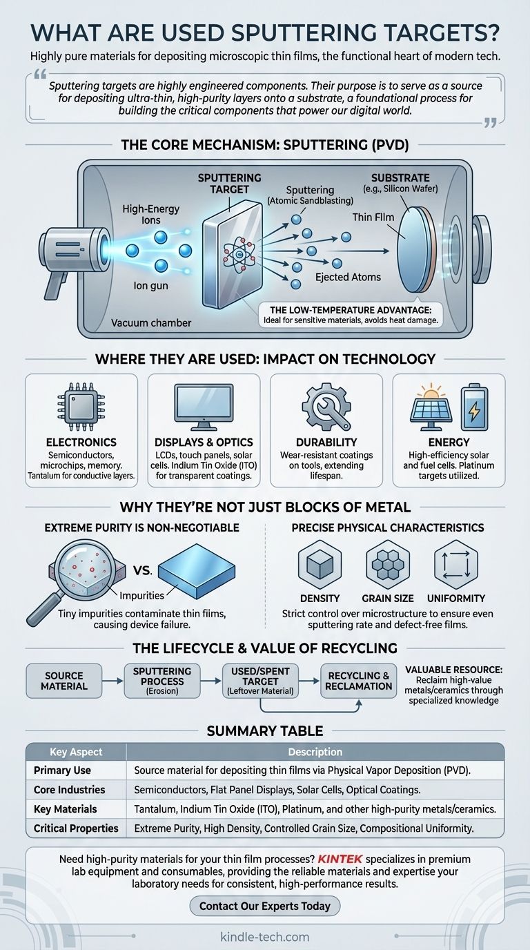
Sputtering targets are not just raw materials; they are highly engineered components. Their purpose is to serve as a source for depositing ultra-thin, high-purity layers onto a substrate, a foundational process for building the critical components that power our digital world.
What is Sputtering? A Foundational Process
The Core Mechanism
Sputtering is a physical vapor deposition (PVD) method performed in a vacuum chamber.
Think of it as a form of atomic "sandblasting." High-energy ions are fired at the sputtering target, which is the source material.
When these ions strike the target, they dislodge or "sputter" individual atoms from its surface. These ejected atoms then travel through the vacuum and deposit onto a substrate (like a silicon wafer or piece of glass), forming an extremely thin and uniform film.
The Low-Temperature Advantage
One of the key advantages of this process is its ability to operate at very low temperatures. This makes it ideal for depositing films onto sensitive materials that would be damaged by high-heat methods.
Where Sputtering Targets Are Used: The Impact on Technology
The thin films created through sputtering are essential to a vast range of industries. The specific material of the target dictates the properties of the final film.
The Heart of Modern Electronics
Sputtering is fundamental to the semiconductor industry. It is used to produce microchips, memory chips, print heads, and flat panel displays.
Tantalum sputtering targets, for example, are commonly used to create the microscopic conductive layers within these essential components.
The Science of Seeing: Displays and Optics
This process is critical for creating transparent conductive coatings for displays.
Indium Tin Oxide (ITO) targets are used to make these coatings for LCDs, touch panels, and plasma displays. The same ITO films are also used in solar cells and for creating antistatic coatings.
Enhancing Durability and Function
Sputtering is used to apply hard, wear-resistant coatings to tools and other industrial components, significantly extending their lifespan.
Specialized targets are also used in energy applications. For example, sputtered platinum targets have widespread applications in the manufacturing of high-efficiency solar cells and fuel cells.
Why Sputtering Targets Are Not Just Blocks of Metal
The performance of the final product depends entirely on the quality of the sputtered film, which in turn depends on the quality of the target. These targets have far higher requirements than traditional materials.
Extreme Purity is Non-Negotiable
Targets must have exceptional purity. Even tiny amounts of impurities can contaminate the thin film, altering its electrical or optical properties and causing the final device to fail.
Precise Physical Characteristics
Beyond purity, targets require strict control over their physical makeup. This includes density, grain size, and compositional uniformity.
Defects like voids or inconsistent grain structure within the target can lead to an uneven sputtering rate, resulting in a flawed and useless thin film.
The Lifecycle of a Sputtering Target
From Source to "Used" Material
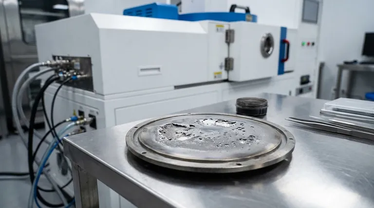
During the sputtering process, atoms are ejected from the surface of the target, gradually eroding it. However, the process is not 100% efficient, and a significant amount of the expensive target material is always left over.
This leftover material is what is known as a used or spent sputtering target.
The Value in Recycling
Because sputtering targets are made of valuable and highly refined metals, they are prime candidates for recycling.
Properly handling and processing these used targets requires specialized knowledge to reclaim the maximum value from the leftover material, ensuring it can be refined and used again.
Making the Right Choice for Your Goal
- If your primary focus is on electronics manufacturing: Understand that sputtering is a fundamental deposition technique, and the quality of the sputtering target directly determines the performance and reliability of your microchips and displays.
- If your primary focus is on materials science: Recognize that the value of a sputtering target lies in its extreme purity and precisely controlled microstructure, which are necessary to produce consistent, high-performance thin films.
- If your primary focus is on supply chain or sustainability: Acknowledge that used sputtering targets are a valuable resource, and establishing a robust recycling program is crucial for cost control and resource management.
Ultimately, sputtering targets are the unseen, high-purity sources that enable the creation of the microscopic layers that make modern technology possible.
Summary Table:
| Key Aspect | Description |
|---|---|
| Primary Use | Source material for depositing thin films via Physical Vapor Deposition (PVD). |
| Core Industries | Semiconductors, Flat Panel Displays, Solar Cells, Optical Coatings. |
| Key Materials | Tantalum, Indium Tin Oxide (ITO), Platinum, and other high-purity metals/ceramics. |
| Critical Properties | Extreme Purity, High Density, Controlled Grain Size, Compositional Uniformity. |
Need high-purity materials for your thin film processes? KINTEK specializes in premium lab equipment and consumables, providing the reliable materials and expertise your laboratory needs for consistent, high-performance results. Contact our experts today to discuss your specific application and ensure your success.
Visual Guide
Related Products
- RF PECVD System Radio Frequency Plasma-Enhanced Chemical Vapor Deposition RF PECVD
- Aluminized Ceramic Evaporation Boat for Thin Film Deposition
- Custom PTFE Wafer Holders for Lab and Semiconductor Processing
- Vacuum Hot Press Furnace Machine for Lamination and Heating
- Precision Machined Zirconia Ceramic Ball for Engineering Advanced Fine Ceramics
People Also Ask
- What is the principle of plasma enhanced chemical vapor deposition? Achieve Low-Temperature Thin Film Deposition
- What is plasma activated chemical vapour deposition method? A Low-Temperature Solution for Advanced Coatings
- What are the advantages of PECVD? Enable Low-Temperature, High-Quality Thin-Film Deposition
- What is an example of PECVD? RF-PECVD for High-Quality Thin Film Deposition
- How are PECVD and CVD different? A Guide to Choosing the Right Thin-Film Deposition Process