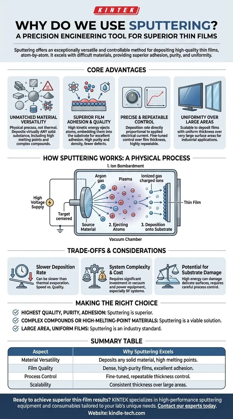
In materials science and manufacturing, sputtering is used because it provides an exceptionally versatile and controllable method for depositing high-quality thin films onto a surface. It excels at coating materials that are difficult or impossible to handle with other techniques, like those with very high melting points. The process results in films with superior adhesion, purity, and uniformity, making it a critical technology in industries from semiconductors to optics.
Sputtering is not just another coating method; it is a precision engineering tool. We use it because it physically transfers material atom-by-atom, offering unparalleled control and the ability to work with virtually any solid material, ensuring the final film is dense, pure, and strongly bonded to its substrate.
The Core Advantages of Sputtering
To understand why sputtering is so widely adopted, it's essential to look at the specific problems it solves better than alternative thin-film deposition methods.
Unmatched Material Versatility
Sputtering is a physical process, not a chemical or thermal one. This distinction is the source of its primary strength.
Because it doesn't rely on melting or evaporating the source material, it can be used to deposit virtually any solid substance. This includes metals, semiconductors, insulators, complex compounds, and mixtures.
This makes it the go-to method for materials with extremely high melting points or low vapor pressure, which are unsuitable for thermal evaporation.
Superior Film Adhesion and Quality
The atoms ejected from the sputtered target have significantly higher kinetic energy than those from an evaporated source.
This high energy causes the atoms to embed themselves slightly into the substrate surface, creating an interfacial diffusion layer. The result is excellent adhesion between the film and the substrate.
Furthermore, because the process doesn't involve boiling a source material, it avoids contamination from the crucible. This leads to films of high purity, high density, and fewer pinhole defects.
Precise and Repeatable Control
The rate of deposition in a sputtering system is directly proportional to the electrical current applied to the target.
This relationship allows for fine-tuned control over film thickness and growth rate. Once a process is established, it is highly repeatable, ensuring consistent results from one run to the next.
Uniformity Over Large Areas
Sputtering systems can be engineered to deposit films of uniform thickness over very large surface areas. This scalability is crucial for industrial applications, from coating architectural glass to manufacturing flat-panel displays.
How Sputtering Works: A Physical Process
Understanding the mechanism reveals why these advantages are possible. It is a process of momentum transfer, much like a cue ball breaking a rack of billiard balls.
The Concept of Ion Bombardment
The process takes place in a vacuum chamber filled with an inert gas, typically Argon. A high voltage is applied to the source material (the "target").
This voltage ionizes the gas, creating a plasma of positively charged ions. These ions are accelerated by the electric field and collide with the negatively charged target at high speed.
Ejecting Atoms, Not Melting Them
When an energetic ion strikes the target, its momentum is transferred to the atoms of the target material, knocking them loose.
These ejected atoms travel through the vacuum chamber until they strike the object being coated (the "substrate").
Deposition onto the Substrate
Upon arrival, the sputtered atoms condense on the substrate, gradually building up a thin, dense, and uniform film.
Understanding the Trade-offs and Considerations
No technology is perfect for every scenario. Sputtering has specific trade-offs that are important to recognize.
Deposition Rate
In many cases, sputtering is a slower deposition process compared to thermal evaporation. For applications where speed is the only priority and film quality is secondary, other methods may be more economical.
System Complexity and Cost
Sputtering systems, especially those using Radio Frequency (RF) power supplies for insulating materials, can be complex and expensive to acquire and maintain. While DC sputtering is more cost-effective, the overall technology requires a significant investment in vacuum and power-delivery equipment.
Potential for Substrate Damage
The high energy of the process, while excellent for adhesion, can sometimes cause damage to extremely delicate or sensitive substrates. Careful process control is required to mitigate this risk in applications like advanced semiconductor manufacturing.
Making the Right Choice for Your Application
Choosing a deposition method depends entirely on your project's specific goals and constraints.
- If your primary focus is the highest film quality, purity, and adhesion: Sputtering is often the superior choice due to the energetic nature of the deposition.
- If your primary focus is coating complex compounds or high-melting-point materials: Sputtering is one of the few viable, and often the only, practical solution.
- If your primary focus is coating large areas with a uniform, decorative, or functional film: The scalability and control of sputtering make it an industry standard for optics, packaging, and electronics.
Ultimately, sputtering is chosen when the integrity, performance, and precision of the final thin film cannot be compromised.
Summary Table:
| Aspect | Why Sputtering Excels |
|---|---|
| Material Versatility | Deposits any solid material, including those with very high melting points. |
| Film Quality | Produces dense, high-purity films with excellent adhesion and uniformity. |
| Process Control | Offers fine-tuned, repeatable control over film thickness and growth rate. |
| Scalability | Capable of coating large surface areas with consistent thickness. |
Ready to achieve superior thin-film results for your lab?
At KINTEK, we specialize in providing high-performance sputtering equipment and consumables tailored to your laboratory's unique needs. Whether you are developing next-generation semiconductors, precision optics, or advanced coatings, our solutions deliver the unmatched material versatility, film quality, and process control detailed in this article.
Contact our experts today to discuss how our sputtering technology can enhance your research and manufacturing processes.
Visual Guide
Related Products
- Spark Plasma Sintering Furnace SPS Furnace
- Vacuum Induction Melting Spinning System Arc Melting Furnace
- Chemical Vapor Deposition CVD Equipment System Chamber Slide PECVD Tube Furnace with Liquid Gasifier PECVD Machine
- Customer Made Versatile CVD Tube Furnace Chemical Vapor Deposition Chamber System Equipment
- Vacuum Cold Mounting Machine for Sample Preparation
People Also Ask
- What is the mechanism of SPS process? A Deep Dive into Rapid, Low-Temperature Sintering
- What are the advantages of CAMI/SPS for W-Cu composite preparation? Reduce cycles from hours to seconds.
- Why are Spark Plasma Sintering (SPS) furnaces or hot presses utilized in the preparation of Li3PS4 solid electrolytes?
- What are the fundamentals of spark plasma sintering process? Unlock Rapid, High-Performance Material Consolidation
- What is the theory of spark plasma sintering? A Guide to Rapid, Low-Temperature Densification


