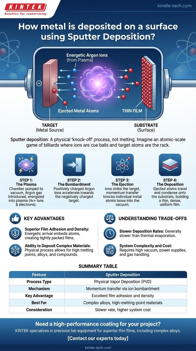
In short, sputter deposition is a physical process where individual atoms are ejected from a solid metal source, called a target, by bombarding it with high-energy ions. These ejected atoms then travel through a vacuum and condense onto a surface, called a substrate, building up a thin, uniform film atom by atom.
Sputter deposition is best understood as a physical "knock-off" process, not a melting one. Imagine an atomic-scale game of billiards where energetic ions are the cue balls, striking a rack of target atoms and sending them flying toward the substrate.
The Core Mechanism: An Atomic Billiards Game
Sputter deposition is a type of Physical Vapor Deposition (PVD) that relies on momentum transfer, making it a highly controlled and versatile technique. The process unfolds in a few distinct steps inside a vacuum chamber.
Step 1: Creating the "Ammunition" - The Plasma
First, the chamber is pumped down to a high vacuum to remove any contaminants. A small amount of an inert gas, most commonly Argon, is then introduced.
A strong electric field is applied, which energizes the Argon gas and strips electrons from its atoms. This creates a glowing, energized state of matter called a plasma, which consists of positively charged Argon ions and free electrons.
Step 2: The Bombardment - Aiming at the Target
The source material, a solid block of the metal you want to deposit, is set up as the target. This target is given a negative electrical charge.
The positively charged Argon ions from the plasma are naturally attracted to and accelerate violently towards the negatively charged target. They bombard its surface with significant kinetic energy.
Step 3: The Ejection - Knocking Atoms Loose
This is the "sputtering" event. When an Argon ion strikes the target, it doesn't melt it. Instead, it transfers its momentum to the target atoms, much like a cue ball breaking a rack in billiards.
This collision has enough energy to physically knock individual atoms loose from the target's surface, ejecting them into the vacuum chamber.
Step 4: The Deposition - Building the Film
The ejected metal atoms now travel in a straight line through the low-pressure environment until they strike a surface. That surface is your component, known as the substrate.
Upon hitting the substrate, the atoms condense and stick, forming a thin, dense, and highly uniform film. This process is repeated billions of times, building up the coating layer by layer.
Key Advantages of Sputtering
Understanding the mechanism reveals why sputtering is a preferred method for many high-performance applications.
Superior Film Adhesion and Density
The sputtered atoms arrive at the substrate with considerable energy, much more than in thermal evaporation. This energy allows them to embed slightly into the surface and arrange themselves into a denser, more tightly packed film with excellent adhesion.
Ability to Deposit Complex Materials
Because sputtering is a physical, non-thermal process, it can deposit materials with very high melting points, as well as complex alloys and compounds. The composition of the sputtered film remains very close to the composition of the original target material.
Understanding the Trade-offs
No process is perfect. Sputtering offers precision and quality but comes with its own set of considerations.
Slower Deposition Rates
Generally, sputtering is a slower process compared to thermal evaporation. For applications where speed is the only priority and film quality is secondary, other methods might be chosen.
System Complexity and Cost
Sputtering systems, with their need for high-vacuum pumps, power supplies, and gas handling, are more complex and expensive than simpler PVD methods.
Potential for Substrate Heating
While the process itself is non-thermal, the constant bombardment of energetic atoms can gradually heat the substrate. For extremely temperature-sensitive substrates, this requires careful process control or active cooling.
How to Apply This to Your Project
Choosing a deposition method depends entirely on the required properties of the final film.
- If your primary focus is high-purity, dense films with excellent adhesion: Sputter deposition is the superior choice for creating robust, high-performance coatings.
- If your primary focus is depositing complex alloys or compounds: Sputtering is often the only reliable method to ensure the film's composition matches the source material.
- If your primary focus is rapid coating of a simple metal with less stringent quality demands: A process like thermal evaporation may be a more cost-effective and faster alternative.
Ultimately, sputter deposition gives you precise, atomic-level control over the creation of advanced thin films.
Summary Table:
| Feature | Sputter Deposition |
|---|---|
| Process Type | Physical Vapor Deposition (PVD) |
| Mechanism | Momentum transfer via ion bombardment |
| Key Advantage | Excellent film adhesion and density |
| Best For | Complex alloys, high-melting-point materials |
| Consideration | Slower deposition rate, higher system cost |
Need a high-performance coating for your project?
KINTEK specializes in precision lab equipment, including sputter deposition systems, to help you achieve superior thin films with excellent adhesion and purity. Our expertise ensures you get the right solution for depositing complex alloys and high-melting-point materials.
Contact our experts today to discuss how our sputtering technology can enhance your research or production process.
Visual Guide
Related Products
- Chemical Vapor Deposition CVD Equipment System Chamber Slide PECVD Tube Furnace with Liquid Gasifier PECVD Machine
- HFCVD Machine System Equipment for Drawing Die Nano-Diamond Coating
- RF PECVD System Radio Frequency Plasma-Enhanced Chemical Vapor Deposition RF PECVD
- 915MHz MPCVD Diamond Machine Microwave Plasma Chemical Vapor Deposition System Reactor
- Customer Made Versatile CVD Tube Furnace Chemical Vapor Deposition Chamber System Equipment
People Also Ask
- Why is Chemical Vapor Deposition (CVD) equipment uniquely suited for constructing hierarchical superhydrophobic structures?
- What is plasma enhanced chemical vapor deposition PECVD equipment? A Guide to Low-Temperature Thin Film Deposition
- What happens during deposition chemistry? Building Thin Films from Gaseous Precursors
- How expensive is chemical vapor deposition? Understanding the True Cost of High-Performance Coating
- What are the advantages of chemical vapor deposition? Achieve Superior Thin Films for Your Lab


