While an indispensable technique for high-quality thin films, sputtering is not without its significant drawbacks. The primary disadvantages are its relatively slow deposition rates, high initial equipment cost, and the potential for substrate heating and material damage from the high-energy process. It also introduces unique challenges regarding film contamination and material limitations.
Sputtering is a process that prioritizes film quality, adhesion, and material versatility over raw speed and low cost. Its disadvantages are fundamentally the trade-offs required to achieve this precision, which can be mitigated—but not eliminated—by more advanced and expensive sputtering techniques.
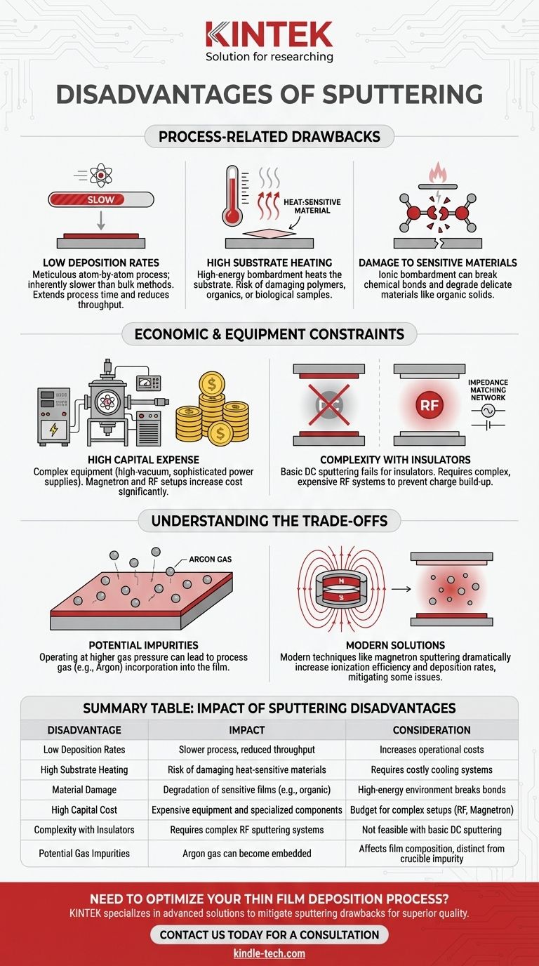
Process-Related Drawbacks
The core physics of sputtering gives rise to several inherent limitations that must be managed.
Low Deposition Rates
Sputtering is an atom-by-atom physical process. This meticulous layering results in high-quality films but is inherently slower than bulk processes like thermal evaporation.
The deposition rates for some materials, particularly oxides and nitrides like SiO2, are notoriously low. This extends process time, which in turn increases operational costs and reduces throughput in a production environment.
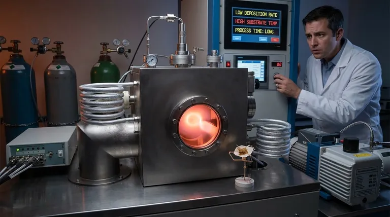
High Substrate Heating
The substrate is bombarded by high-energy particles, including sputtered atoms from the target and ions from the plasma. This energy transfer inevitably heats the substrate.
This heating can be detrimental to heat-sensitive materials, such as polymers, organic electronics, or biological samples. While substrate cooling systems can be implemented, they add to the system's cost and complexity.
Damage to Sensitive Materials
The same ionic bombardment that sputters the target can also damage the growing film and the substrate itself.
This is a critical issue for materials with delicate chemical structures, like organic solids. The high-energy plasma environment can easily break chemical bonds and degrade the material, rendering the deposited film useless.
Economic and Equipment Constraints
Beyond the physics, sputtering presents significant practical and financial hurdles.
High Capital Expense
Sputtering systems are complex and expensive. The required equipment includes a high-vacuum chamber, precise gas flow controllers, and sophisticated power supplies.
The costs escalate further for more advanced setups. For example, magnetron sputtering, which increases deposition rates, and RF sputtering, which is necessary for insulating materials, require more specialized and costly components.
Sputtering Insulators Adds Complexity
Basic DC (Direct Current) sputtering cannot be used to deposit electrically insulating materials. A positive charge builds up on the insulator target surface, repelling the sputtering gas ions and stopping the process.
To overcome this, RF (Radio Frequency) sputtering is required. This involves more complex and expensive power supplies and impedance-matching networks, significantly increasing the overall system cost.
Understanding the Trade-offs
Choosing a deposition method requires weighing the pros and cons. The disadvantages of sputtering are often the necessary price for its unique advantages.
The Myth of Absolute Purity
Compared to thermal evaporation, sputtering has a greater tendency to introduce certain impurities into the film. Because sputtering operates at a higher gas pressure, atoms of the sputtering gas (typically Argon) can become embedded in the growing film.
However, sputtering avoids contamination from a heated crucible, which can be a problem in evaporation. The trade-off is between potential gas incorporation in sputtering versus potential crucible material incorporation in evaporation.
Basic vs. Modern Sputtering
Many of the most cited disadvantages—extremely low rates, low plasma ionization, and severe heating—are most prominent in basic sputtering setups.
Modern techniques like magnetron sputtering were developed specifically to address these issues. By using magnets to confine electrons near the target, magnetrons dramatically increase the ionization efficiency of the plasma, leading to higher deposition rates and reduced substrate heating.
Is Sputtering Right for Your Application?
The decision to use sputtering depends entirely on your project's primary goals and constraints.
- If your primary focus is film quality, density, and adhesion: Sputtering is often the superior choice, but you must budget for the higher equipment costs and longer process times.
- If your primary focus is high-speed, low-cost deposition: A technique like thermal evaporation may be a better fit, provided its lower film density and adhesion are acceptable for your application.
- If you are working with heat-sensitive or organic materials: You must carefully evaluate substrate cooling options and confirm that the sputtering process itself is not too destructive for your material's integrity.
- If you need to deposit a wide variety of materials, including alloys and insulators: Sputtering offers unmatched versatility, but depositing insulators will require investment in a more complex RF sputtering system.
Ultimately, understanding these disadvantages allows you to leverage sputtering's powerful strengths for applications where quality and material performance cannot be compromised.
Summary Table:
| Disadvantage | Impact |
|---|---|
| Low Deposition Rates | Slower process time, reduced throughput |
| High Substrate Heating | Risk of damaging heat-sensitive materials |
| Material Damage | High-energy ions can degrade sensitive films |
| High Capital Cost | Expensive vacuum chambers and power supplies |
| Complexity with Insulators | Requires RF sputtering for non-conductive materials |
| Potential Gas Impurities | Argon gas can become embedded in the film |
Need to optimize your thin film deposition process? At KINTEK, we specialize in advanced lab equipment solutions for precise material coating challenges. Our sputtering systems are designed to mitigate common drawbacks like substrate heating and contamination, delivering superior film quality and adhesion for your research or production needs. Let our experts help you select the right equipment for your specific application—contact us today to discuss your project requirements!
Visual Guide
Related Products
- Spark Plasma Sintering Furnace SPS Furnace
- Vacuum Induction Melting Spinning System Arc Melting Furnace
- Chemical Vapor Deposition CVD Equipment System Chamber Slide PECVD Tube Furnace with Liquid Gasifier PECVD Machine
- Customer Made Versatile CVD Tube Furnace Chemical Vapor Deposition Chamber System Equipment
People Also Ask
- What is the process fundamentals of spark plasma sintering? Achieve Rapid, High-Density Material Consolidation
- What is the mechanism of SPS process? A Deep Dive into Rapid, Low-Temperature Sintering
- What is SPS sintering method? A Guide to High-Speed, High-Performance Material Fabrication
- What are the fundamentals of spark plasma sintering process? Unlock Rapid, High-Performance Material Consolidation
- What is the pressure for spark plasma sintering? A Guide to Optimizing SPS Parameters


