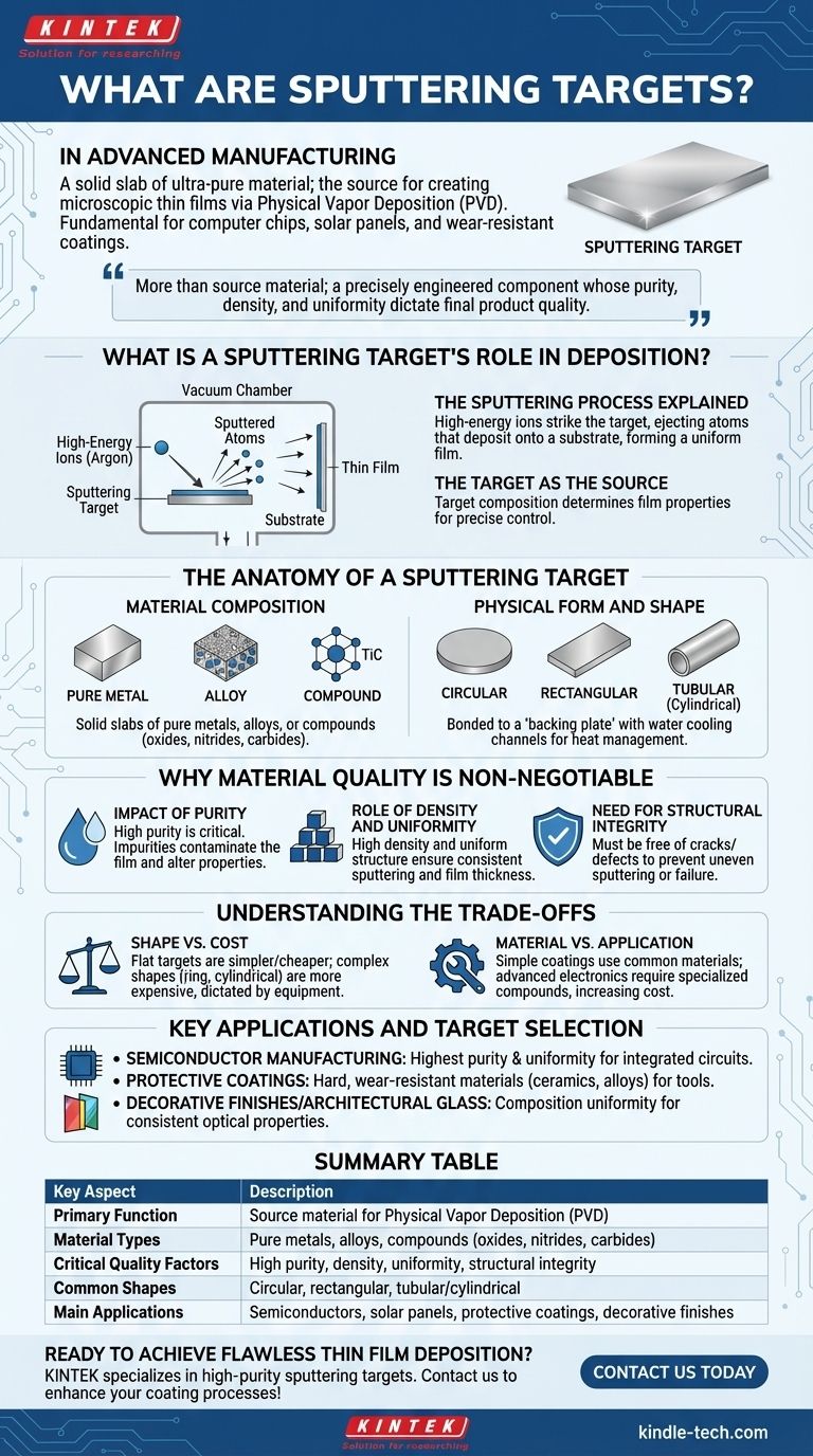
In the world of advanced manufacturing, a sputtering target is a solid slab of ultra-pure material that acts as the source for creating microscopic thin films on surfaces. This process, a form of physical vapor deposition (PVD), is fundamental to producing everything from computer chips and solar panels to wear-resistant coatings on cutting tools.
A sputtering target is more than just a source material; it's a precisely engineered component whose exceptional purity, density, and uniformity are critical for depositing high-performance thin films. The quality of the target directly dictates the quality and reliability of the final product.
What is a Sputtering Target's Role in Deposition?
The Sputtering Process Explained
Think of the sputtering process as sandblasting at an atomic level. In a vacuum chamber, high-energy ions (typically from an inert gas like Argon) are accelerated and aimed at the sputtering target.
When these ions strike the target, they physically knock off, or "sputter," individual atoms or molecules from the target's surface. These ejected particles then travel through the vacuum and deposit onto a substrate (the object being coated), forming a thin, highly uniform film.
The Target as the Source
The sputtering target is the source of these atoms. The composition of the target material determines the exact composition of the film that is created on the substrate. This allows for precise control over the properties of the final coating.
The Anatomy of a Sputtering Target
Material Composition: The Building Blocks
Sputtering targets are manufactured from a wide range of materials, depending on the desired properties of the thin film.
They are typically solid slabs made of pure metals, alloys, or compounds such as oxides, nitrides, or carbides (e.g., Titanium Carbide - TiC).
Physical Form and Shape
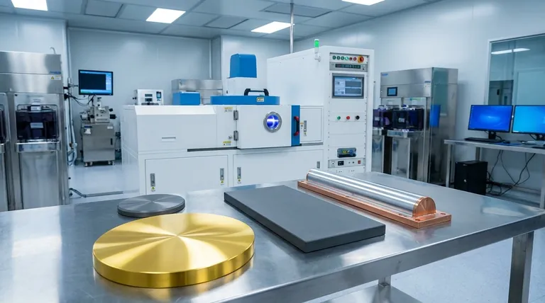
The physical form of a target is designed to fit specific sputtering equipment. Common configurations include circular, rectangular, and tubular (cylindrical) shapes.
Targets are typically bonded to a metallic holder, often called a "backing plate," which includes channels for water cooling to manage the intense heat generated during the sputtering process.
Why Material Quality is Non-Negotiable
Sputtering targets are held to far higher standards than traditional industrial materials. This is because even minuscule imperfections in the target will be transferred to the thin film, compromising the final product's performance.
The Impact of Purity
High purity is the most critical requirement. Any impurity atoms within the target can be sputtered along with the primary material, contaminating the thin film and altering its electrical, optical, or mechanical properties.
The Role of Density and Uniformity
A target must have high density and a uniform grain structure. This ensures a consistent and predictable sputtering rate across the entire surface, leading to a film with uniform thickness and composition.
The Need for Structural Integrity
The material must be completely free of cracks and defects. Such flaws can cause uneven sputtering, introduce contaminants into the vacuum chamber, or even lead to the target failing under the stress of the process.
Understanding the Trade-offs
Shape vs. Cost
The complexity of a target's shape directly influences its cost. Flat targets are generally simpler and less expensive to manufacture and replace.
However, some equipment designs require more complex forms like ring-shaped or cylindrical targets, which are more expensive to produce. The choice is dictated by the sputtering system, not user preference.
Material vs. Application
The intended application determines the necessary material. Simple protective or decorative coatings may use common metals or alloys.
Conversely, advanced applications in the electronics or information industry demand highly specialized compound materials with specific properties, which increases manufacturing complexity and cost.
Key Applications and Target Selection
- If your primary focus is semiconductor manufacturing: You require targets with the absolute highest purity and uniformity to create reliable integrated circuits and electronic components.
- If your primary focus is creating protective coatings: You will select targets made of hard, wear-resistant materials like ceramics (TiC, BN) or specific corrosion-resistant alloys for tools and equipment.
- If your primary focus is decorative finishes or architectural glass: Composition uniformity is key to ensure consistent color, reflectivity, and optical properties across the entire coated surface.
Ultimately, selecting the right sputtering target is a critical engineering decision that defines the performance and quality of the final coated product.
Summary Table:
| Key Aspect | Description |
|---|---|
| Primary Function | Source material for Physical Vapor Deposition (PVD) |
| Material Types | Pure metals, alloys, compounds (oxides, nitrides, carbides) |
| Critical Quality Factors | High purity, density, uniformity, structural integrity |
| Common Shapes | Circular, rectangular, tubular/cylindrical |
| Main Applications | Semiconductors, solar panels, protective coatings, decorative finishes |
Ready to achieve flawless thin film deposition? KINTEK specializes in high-purity sputtering targets tailored for your laboratory's specific needs. Whether you're in semiconductor manufacturing, solar energy, or advanced materials research, our targets deliver the exceptional purity and uniformity required for reliable results. Contact us today to discuss how our lab equipment and consumables can enhance your coating processes!
Visual Guide
Related Products
- Reference Electrode Calomel Silver Chloride Mercury Sulfate for Laboratory Use
- Multifunctional Electrolytic Electrochemical Cell Water Bath Single Layer Double Layer
- Molybdenum Tungsten Tantalum Special Shape Evaporation Boat
- Hemispherical Bottom Tungsten Molybdenum Evaporation Boat
- Cylindrical Press Mold with Scale for Lab
People Also Ask
- What is the recommended maintenance for the filling solution of a reference electrode? A Guide to Stable & Accurate Readings
- Which electrode is used as a reference electrode for measuring half-cell potentials? Understanding the Universal Standard
- Why is the selection of a high-quality reference electrode critical in the electrochemical synthesis? | KINTEK
- How does the selection of reference electrodes correlate with electrolyte pH in HER testing? Ensure Precise Potential
- What is the purpose of the reference electrode? Achieve Stable & Accurate Electrochemical Measurements


