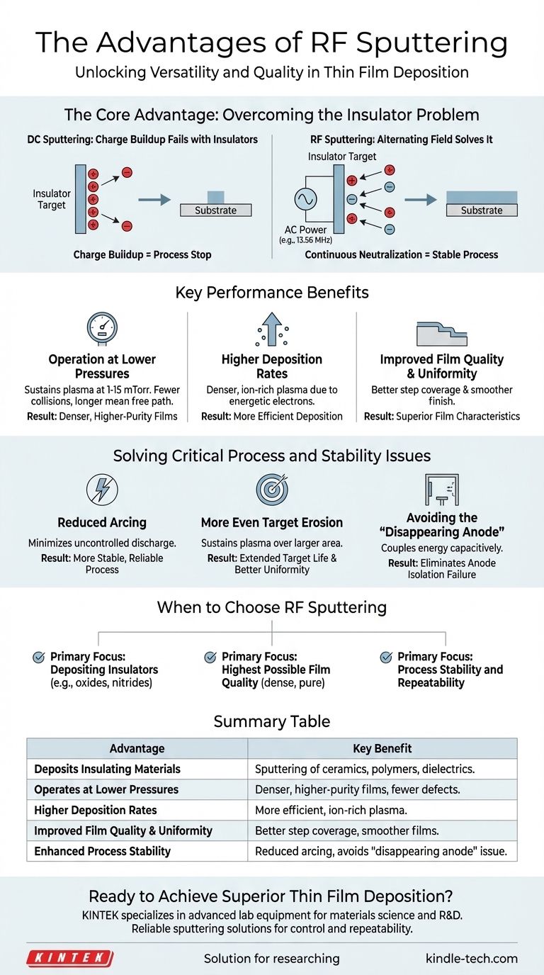
The fundamental advantage of RF sputtering is its unique ability to deposit thin films from non-conductive, or insulating, materials. While traditional DC sputtering is limited to conductive targets, the use of a radio frequency power source overcomes this restriction, making it possible to deposit a vast range of ceramics, polymers, and other dielectrics with high quality and control.
The core value of RF sputtering lies in its alternating electric field. This simple change from direct current (DC) to alternating current (AC) prevents electrical charge from accumulating on insulating targets, solving the critical failure point of DC systems and unlocking a more versatile, stable, and efficient deposition process.
The Core Advantage: Overcoming the Insulator Problem
The most significant distinction between RF and DC sputtering is how they handle electrical charge. This difference is the primary reason RF sputtering was developed and remains essential for modern materials science.
How DC Sputtering Fails with Insulators
In standard DC sputtering, a high negative DC voltage is applied to the target material. This attracts positively charged gas ions (like Argon+) from the plasma, which strike the target and physically eject, or "sputter," atoms.
This process works perfectly for conductive metal targets, which can easily dissipate the positive charge delivered by the ions.
However, if the target is an insulator (like quartz or a ceramic), the positive charge from the impacting ions cannot flow away. This charge buildup quickly neutralizes the negative voltage on the target, repelling any more positive ions and effectively shutting down the sputtering process.
How RF Sputtering Solves It
RF sputtering replaces the constant DC voltage with a high-frequency alternating voltage, typically at 13.56 MHz.
During one half of the AC cycle, the target is negative, attracting ions and causing sputtering just like in the DC process.
Crucially, during the other half of the cycle, the target becomes positive. This attracts a flood of highly mobile electrons from the plasma, which neutralize the positive charge that built up during the sputtering phase. This continuous neutralization prevents charge buildup and allows the sputtering of insulators to proceed indefinitely.
Key Performance Benefits of RF Sputtering
Beyond its ability to handle insulators, the use of an RF field creates a more efficient and controllable plasma environment, leading to tangible performance gains.
Operation at Lower Pressures
RF energy is very effective at sustaining a plasma. This allows RF sputtering systems to operate at significantly lower gas pressures (typically 1-15 mTorr) compared to DC sputtering (often near 100 mTorr).
Operating at lower pressure means there are fewer gas atoms between the target and the substrate. This increases the mean free path, allowing sputtered atoms to travel in a more direct line to the substrate with fewer energy-losing collisions, resulting in denser and higher-purity films.
Higher Deposition Rates
The oscillating electrons in the RF plasma are more energetic and follow longer paths, increasing the probability of them colliding with and ionizing neutral gas atoms.
This creates a denser, more ion-rich plasma compared to a simple DC discharge at the same pressure. A higher density of ions striking the target leads directly to higher sputtering rates and a more efficient deposition process.
Improved Film Quality and Uniformity
The combination of lower operating pressure and a stable, arc-free process contributes to superior film characteristics. The more direct path of sputtered atoms leads to better step coverage over complex surface topographies and a smoother, more uniform final film.
Solving Critical Process and Stability Issues
RF sputtering inherently solves several common problems that can plague DC sputtering systems, leading to a more robust and repeatable manufacturing process.
Reduced Arcing
Arcing is a sudden, uncontrolled electrical discharge that can occur when charge builds up on a surface. In DC systems, this is a common issue, especially with any slight contamination or oxidation on the target. These arcs can damage the substrate and create defects in the growing film.
Because the RF field actively neutralizes surface charge every cycle, the potential for arcing is dramatically reduced, leading to a much more stable process.
More Even Target Erosion
Many DC systems use magnets to confine the plasma near the target surface, which increases efficiency but concentrates the sputtering in a narrow band. This creates a deep "racetrack" groove, wasting much of the target material outside this area.
RF sputtering can sustain a plasma over a larger portion of the target face. Advanced RF Diode sputtering technologies further improve this, enabling very flat target erosion, which extends the life of the target and improves coating uniformity.
Avoiding the "Disappearing Anode"
In DC systems, the chamber walls often serve as the anode (the positive terminal). Over time, insulating material can get sputtered onto the walls, electrically isolating the anode from the plasma. This "disappearing anode" effect can destabilize or extinguish the plasma.
RF sputtering couples energy into the plasma capacitively, without relying on a direct conductive path to a fixed anode, thus avoiding this failure mode entirely.
When to Choose RF Sputtering
Your choice of deposition technology should be guided by your material requirements and performance goals.
- If your primary focus is depositing insulators: RF sputtering is not just an advantage; it is a necessity. This includes materials like oxides (SiO₂, Al₂O₃), nitrides, and other ceramics.
- If your primary focus is the highest possible film quality: The low-pressure operation of RF sputtering provides a key advantage for creating dense, pure films with excellent step coverage.
- If your primary focus is process stability and repeatability: RF sputtering's inherent resistance to arcing and process drift makes it a more reliable choice for demanding production environments.
Ultimately, RF sputtering empowers you to work with a far broader palette of materials while achieving a more stable and controlled deposition process.
Summary Table:
| Advantage | Key Benefit |
|---|---|
| Deposits Insulating Materials | Enables sputtering of ceramics, polymers, and other dielectrics. |
| Operates at Lower Pressures | Results in denser, higher-purity films with fewer defects. |
| Higher Deposition Rates | More efficient process due to a denser, more ion-rich plasma. |
| Improved Film Quality & Uniformity | Better step coverage and smoother, more uniform films. |
| Enhanced Process Stability | Dramatically reduced arcing and avoidance of the "disappearing anode" issue. |
Ready to Achieve Superior Thin Film Deposition?
RF sputtering is essential for depositing high-quality films from insulating materials like oxides and ceramics. Whether your focus is on material versatility, film quality, or process stability, the right equipment is critical to your success.
KINTEK specializes in advanced lab equipment and consumables, serving the precise needs of materials science and R&D laboratories. We provide reliable sputtering solutions that deliver the control and repeatability required for your most demanding projects.
Contact us today to discuss how our expertise can enhance your thin film deposition process. Let's find the perfect solution for your laboratory's needs.
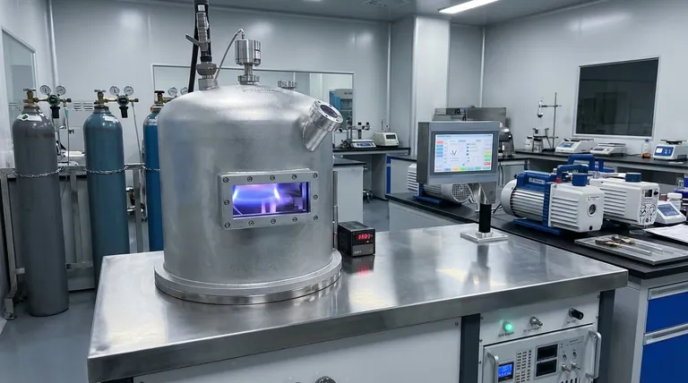
Visual Guide
Related Products
- RF PECVD System Radio Frequency Plasma-Enhanced Chemical Vapor Deposition RF PECVD
- Spark Plasma Sintering Furnace SPS Furnace
- Horizontal High Temperature Graphite Vacuum Graphitization Furnace
People Also Ask
- What is plasma enhanced chemical vapour deposition PECVD used for? Enable Low-Temp Thin Films for Electronics & Solar
- How does plasma enhance CVD? Unlock Low-Temperature, High-Quality Film Deposition
- What is an example of PECVD? RF-PECVD for High-Quality Thin Film Deposition
- What is plasma enhanced chemical vapour deposition process? Unlock Low-Temperature, High-Quality Thin Films
- What is plasma CVD? Unlock Low-Temperature Thin Film Deposition for Sensitive Materials


