In short, sputtering is a foundational technology used to deposit ultra-thin, high-performance films of material onto a surface. Its applications are vast, spanning from the creation of microchips in semiconductor manufacturing and anti-reflection coatings on eyeglasses to durable, wear-resistant coatings on cutting tools and decorative finishes on consumer products.
The core value of sputtering is not a single application, but its exceptional versatility and control. It allows engineers to deposit a wide range of materials with high purity, density, and adhesion, making it an essential process for creating advanced electronic, optical, and mechanical components.

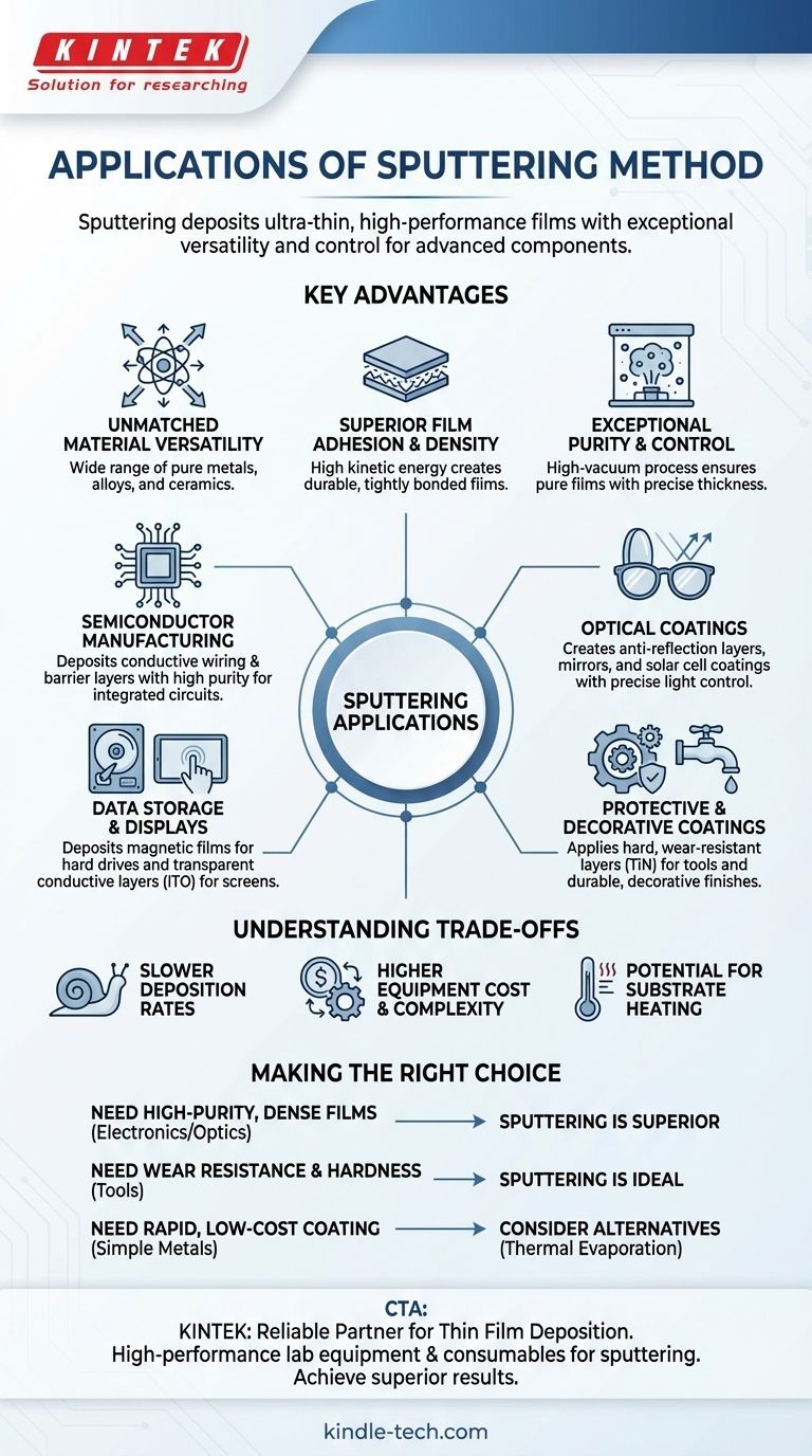
Why Sputtering is So Widely Used
The sputtering process, which involves bombarding a target material with energized ions in a vacuum, provides several distinct advantages. These benefits are the direct reason for its adoption across so many industries.
Unmatched Material Versatility
The physical nature of sputtering—mechanically ejecting atoms from a target—means it can be used with an enormous range of materials. This includes pure metals, alloys, and even insulating ceramic compounds, which are difficult or impossible to deposit using other methods.
Superior Film Adhesion and Density
Atoms ejected from the sputtered target have high kinetic energy. When they strike the substrate (the object being coated), they form an incredibly dense and tightly bonded film with superior adhesion compared to many other coating techniques.
Exceptional Purity and Control
The entire process occurs within a high-vacuum chamber, which is first purged of contaminants and then filled with a high-purity inert gas like Argon. This controlled environment ensures the resulting film is extremely pure. Furthermore, operators can precisely control film thickness and uniformity by managing parameters like gas pressure and power.
Key Application Areas in Detail
The unique advantages of sputtering make it the ideal choice for numerous high-stakes applications where film quality is paramount.
Semiconductor Manufacturing
Sputtering is critical for fabricating integrated circuits. It is used to deposit the thin layers of conductive metals (like aluminum or copper) that form the microscopic wiring connecting transistors, as well as the barrier layers that prevent these metals from diffusing into other parts of the chip. Purity and precision are non-negotiable here.
Optical Coatings
From camera lenses and eyeglasses to architectural glass, sputtering is used to apply anti-reflection coatings. By depositing multiple, precisely controlled layers of materials with different refractive indices, manufacturers can minimize glare and maximize light transmission. It's also used for creating highly reflective mirrors and solar cell coatings.
Data Storage and Displays
The magnetic layers on hard disk drives and other magnetic storage media are deposited using sputtering. This process ensures the creation of a uniform, dense magnetic film capable of storing data reliably. It is also used to deposit the transparent conductive films (like ITO) essential for touch screens and flat-panel displays.
Protective and Decorative Coatings
The dense, hard films created by sputtering are ideal for wear resistance. It is commonly used to coat cutting tools, drills, and industrial components with materials like Titanium Nitride (TiN), dramatically increasing their lifespan. This same durability also lends itself to creating long-lasting decorative finishes on watches, faucets, and other hardware.
Understanding the Trade-offs
No technology is perfect. To make an informed decision, it is crucial to understand the limitations of sputtering.
Slower Deposition Rates
Compared to other methods like thermal evaporation, sputtering is generally a slower process. The rate at which material is ejected from the target is often lower, which can impact throughput in high-volume manufacturing.
Higher Equipment Cost and Complexity
Sputtering systems require sophisticated equipment, including high-vacuum chambers, powerful magnets, and high-voltage power supplies. This results in a higher initial capital investment and more complex operation compared to simpler coating techniques.
Potential for Substrate Heating
The high-energy bombardment inherent in the process can transfer significant heat to the substrate. This can be a concern when coating temperature-sensitive materials, such as certain plastics or biological samples, and may require additional cooling systems.
Making the Right Choice for Your Goal
Selecting the right deposition method depends entirely on the required film properties and project constraints.
- If your primary focus is high-purity, dense films for electronics or optics: Sputtering is often the superior choice due to its precise control over thickness, uniformity, and material purity.
- If your primary focus is wear resistance and hardness for tools or components: The excellent adhesion and density of sputtered films make it an ideal technology for creating durable protective coatings.
- If your primary focus is rapid, low-cost coating of simple metals: You might investigate alternative methods like thermal evaporation, which can offer higher deposition rates and lower equipment complexity.
Ultimately, sputtering is a key enabling technology that has made many of our modern devices and high-performance products possible.
Summary Table:
| Application Area | Key Uses & Benefits |
|---|---|
| Semiconductor Manufacturing | Deposits conductive wiring & barrier layers with high purity and precision for microchips. |
| Optical Coatings | Creates anti-reflection layers for lenses and highly reflective mirrors with precise light control. |
| Data Storage & Displays | Deposits magnetic films for hard drives and transparent conductive layers (ITO) for touch screens. |
| Protective & Decorative Coatings | Applies hard, wear-resistant layers (e.g., TiN) for tools and durable finishes for consumer goods. |
Need a reliable partner for your thin film deposition?
KINTEK specializes in high-performance lab equipment and consumables for sputtering applications. Whether you are developing next-generation semiconductors, precision optics, or durable protective coatings, our solutions deliver the purity, density, and control your research demands.
Contact our experts today to discuss how we can support your laboratory's specific needs and help you achieve superior coating results.
Visual Guide
Related Products
- Lab Sterile Slapping Type Homogenizer for Tissue Mashing and Dispersing
- Spark Plasma Sintering Furnace SPS Furnace
- Single Punch Manual Tablet Press Machine TDP Tablet Punching Machine
People Also Ask
- How do ultrasonic cell disruptors or dispersion equipment function during ZIF-8 synthesis? Master Acoustic Cavitation
- How does a homogenizer affect the quality of electrode slurry? Master Battery Consistency with High-Shear Mixing
- How do lab stirrers & homogenizers ensure uniform distribution? Optimize Your Complex Multiphase Chemical Mixing
- What is the primary function of an ultrasonic cleaner in coating? Achieve Unmatched Substrate Purity for PVD Adhesion
- Why is it necessary to use an ultrasonic cell disruptor before yeast flow cytometry? Ensure Data Accuracy


