Sputtering is a highly versatile vacuum deposition technique used to create ultra-thin films of material across a vast range of high-technology industries. Its primary applications are found in manufacturing semiconductors, optical lenses, data storage devices like hard drives, solar panels, and applying durable or decorative coatings to everything from cutting tools to architectural glass.
The core reason for sputtering's widespread use is its exceptional control. It allows engineers to deposit highly uniform, dense, and pure thin films from virtually any material onto a substrate, a level of precision that is critical for modern electronics and advanced materials.
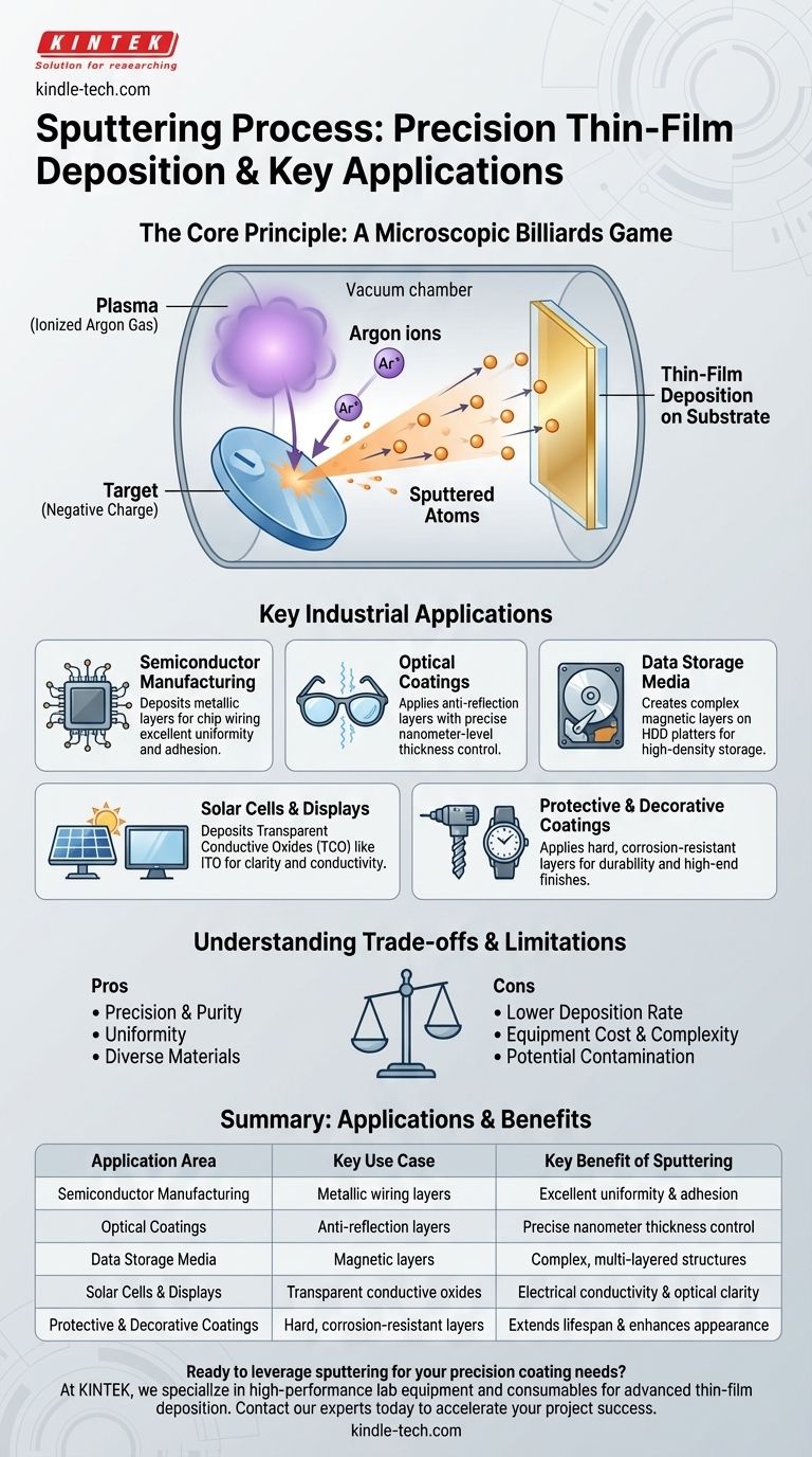
The Core Principle: A Microscopic Billiards Game
To understand sputtering's applications, you must first understand its mechanism. It is fundamentally a physical process, not a chemical one, that takes place inside a vacuum chamber.
Creating the Plasma
The process begins by introducing a small amount of an inert gas, almost always Argon (Ar), into the vacuum chamber. A high voltage is applied, which strips electrons from the argon atoms, creating a glowing, ionized gas known as a plasma.
The Target Bombardment
The material to be deposited, known as the target, is given a negative electrical charge. This attracts the positively charged argon ions from the plasma, which accelerate and collide with the target at high speeds.
Thin-Film Deposition
Each collision acts like a microscopic billiard ball break, knocking loose or "sputtering" atoms from the target material. These ejected atoms travel through the vacuum chamber and land on the substrate (the object being coated), gradually building up a thin, uniform film.
Where Sputtering Excels: Key Industrial Applications
The precise, controllable nature of this process makes it indispensable in fields where material properties at the nanometer scale are critical.
Semiconductor Manufacturing
In the creation of integrated circuits (microchips), sputtering is used to deposit the various metallic layers that form the chip's wiring and connections. The process provides excellent uniformity across the silicon wafer and creates dense films with strong adhesion, which is essential for reliability.
Optical Coatings
Sputtering is the standard method for applying anti-reflection coatings to eyeglass lenses, camera lenses, and other optics. By precisely controlling the film thickness down to the nanometer, manufacturers can fine-tune how the lens interacts with specific wavelengths of light.
Data Storage Media
The magnetic layers on hard disk drive (HDD) platters and other magnetic storage media are deposited using sputtering. This is the only way to create the complex, multi-layered structures with the precise magnetic properties required for high-density data storage.
Solar Cells and Displays
Many solar panels and flat-panel displays (like LCD or OLED screens) require a transparent conductive oxide (TCO) layer. Sputtering is used to deposit materials like Indium Tin Oxide (ITO), which conduct electricity while remaining optically clear.
Protective and Decorative Coatings
Sputtering is used to apply extremely hard, corrosion-resistant coatings to industrial cutting tools, drill bits, and machine parts, significantly extending their lifespan. It is also used for high-end decorative finishes, such as applying metallic sheens to watches, fixtures, or consumer electronics.
Understanding the Trade-offs and Limitations
While powerful, sputtering is not the right solution for every problem. Objectivity requires acknowledging its trade-offs.
Deposition Rate Can Be a Factor
Compared to other methods like thermal evaporation, sputtering can have a lower deposition rate. For applications requiring very thick films or extremely high throughput, this can be a significant limitation.
Equipment Cost and Complexity
Sputtering systems, especially those using Radio Frequency (RF) power supplies for non-conductive materials, are complex and represent a significant capital investment compared to simpler deposition technologies.
Potential for Contamination
The quality of the final film is entirely dependent on the purity of the target material and the vacuum environment. Any impurities in the target can be transferred to the substrate, and residual gases in the chamber can contaminate the film.
Uniformity Challenges at Scale
While excellent for smaller substrates, maintaining perfect film thickness uniformity across very large areas (e.g., cathodes over one meter) can be challenging. This requires sophisticated equipment design to manage the plasma density evenly.
Making the Right Choice for Your Goal
Selecting a deposition method depends entirely on the requirements of the final product.
- If your primary focus is precision, purity, and film quality: Sputtering is the superior choice for creating dense, uniform, and well-adhered films, especially for complex electronics and optics.
- If your primary focus is coating complex alloys or high-melting-point materials: Sputtering excels because it deposits material atom-by-atom without melting the source, allowing for the deposition of materials that are impossible to handle with thermal evaporation.
- If your primary focus is low-cost, high-speed coating: You may need to evaluate simpler methods like thermal evaporation, which can be faster and cheaper for less demanding applications.
Ultimately, understanding the fundamental strengths and weaknesses of the sputtering process empowers you to select the right tool for your specific engineering challenge.
Summary Table:
| Application Area | Key Use Case | Key Benefit of Sputtering |
|---|---|---|
| Semiconductor Manufacturing | Depositing metallic wiring layers on microchips | Excellent uniformity and strong adhesion for reliability |
| Optical Coatings | Applying anti-reflection layers on lenses | Precise nanometer-level thickness control for specific light wavelengths |
| Data Storage Media | Creating magnetic layers on hard drive platters | Ability to form complex, multi-layered structures with precise magnetic properties |
| Solar Cells & Displays | Depositing transparent conductive oxides (e.g., ITO) | Combines electrical conductivity with optical clarity |
| Protective & Decorative Coatings | Applying hard, corrosion-resistant layers on tools and decorative finishes on consumer goods | Creates dense, durable films that extend product lifespan and enhance appearance |
Ready to leverage sputtering for your precision coating needs?
At KINTEK, we specialize in providing high-performance lab equipment and consumables for advanced thin-film deposition. Whether you are developing next-generation semiconductors, optical components, or durable coatings, our sputtering solutions deliver the uniformity, purity, and control your R&D or production requires.
Contact our experts today to discuss how our tailored sputtering systems can enhance your laboratory's capabilities and accelerate your project success.
Visual Guide
Related Products
- Spark Plasma Sintering Furnace SPS Furnace
- Vacuum Induction Melting Spinning System Arc Melting Furnace
- Chemical Vapor Deposition CVD Equipment System Chamber Slide PECVD Tube Furnace with Liquid Gasifier PECVD Machine
- Customer Made Versatile CVD Tube Furnace Chemical Vapor Deposition Chamber System Equipment
People Also Ask
- What is the mechanism of SPS process? A Deep Dive into Rapid, Low-Temperature Sintering
- What is the difference between spark plasma sintering and flash sintering? A Guide to Advanced Sintering Methods
- What is SPS sintering method? A Guide to High-Speed, High-Performance Material Fabrication
- What technical advantages does a Spark Plasma Sintering (SPS) furnace offer for LZP ceramics? Enhance Ionic Conductivity
- What is the theory of spark plasma sintering? A Guide to Rapid, Low-Temperature Densification


