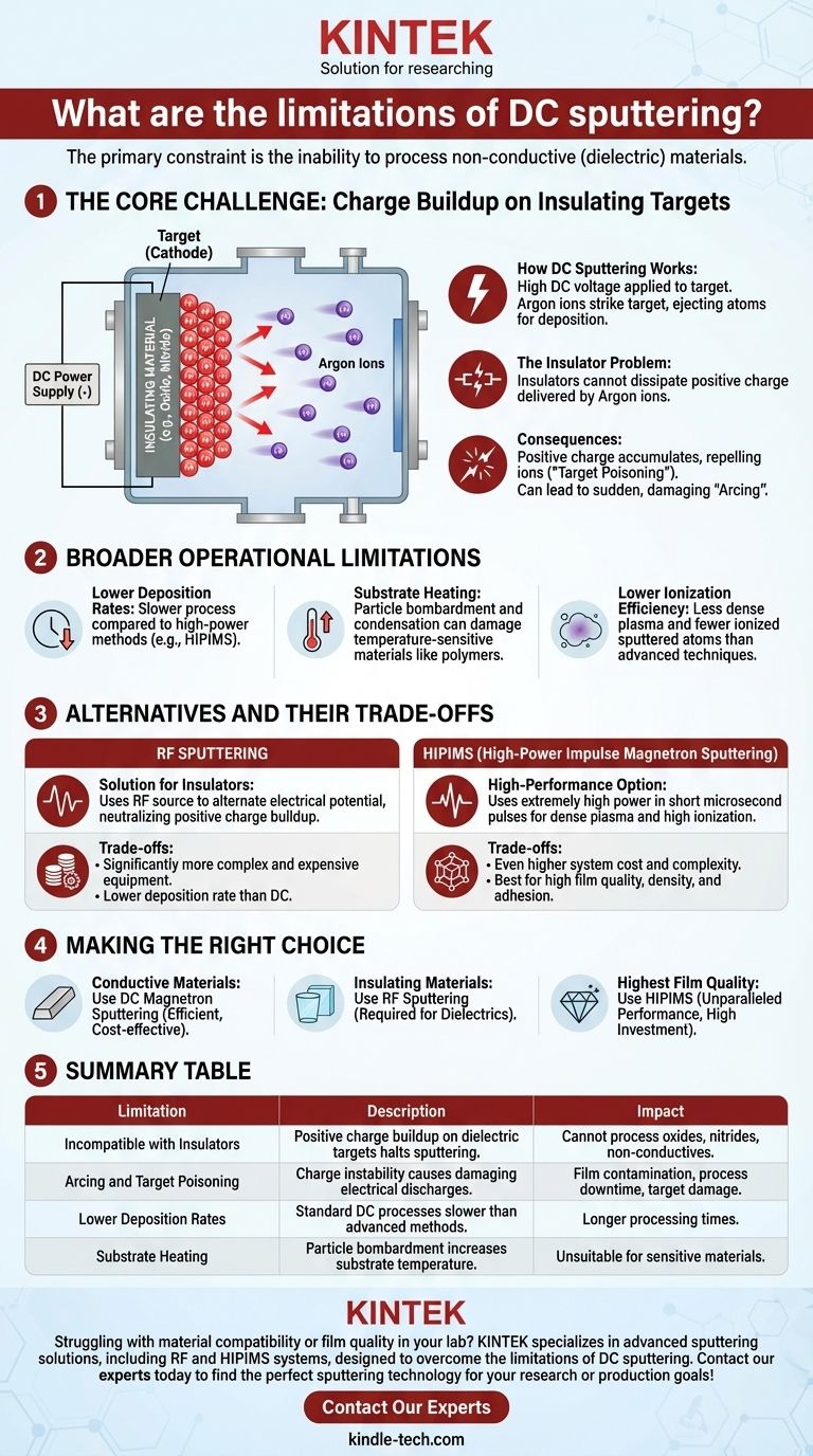
In essence, the primary limitation of DC sputtering is its inability to process non-conductive, or dielectric, materials. This fundamental constraint arises because the direct current process causes a positive electrical charge to build up on the surface of an insulating target. This charge buildup eventually repels the ions used for sputtering, leading to process instability, damaging electrical arcs, and a potential halt to the deposition process altogether.
While DC sputtering is a robust and cost-effective method for depositing conductive films, its reliance on a constant electrical potential makes it fundamentally incompatible with insulating materials. This forces a critical choice between limiting your material selection and adopting more complex and expensive sputtering technologies.
The Core Challenge: Charge Buildup on Insulating Targets
The limitations of DC sputtering are not a fault in the technology but a direct consequence of its underlying physics. Understanding this mechanism is key to selecting the right deposition method.
How DC Sputtering Works
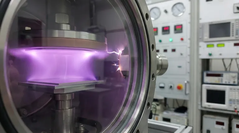
In a standard DC sputtering system, a high DC voltage is applied to the material you wish to deposit, known as the target. This target acts as a cathode (negative electrode).
Inert gas ions, typically Argon, are accelerated from the plasma and strike this negatively charged target. The momentum transfer from this collision ejects, or "sputters," atoms from the target material, which then travel and deposit onto your substrate as a thin film.
The Insulator Problem Explained
This process works flawlessly as long as the target material is electrically conductive. A conductive target can easily dissipate the positive charge delivered by the arriving Argon ions, maintaining its negative potential.
However, if the target is an insulator (like an oxide or nitride), it cannot conduct this charge away. Positive ions accumulate on the target's surface, neutralizing and eventually reversing its polarity to become positive.
Consequences: Arcing and Target Poisoning
Once the target surface becomes positively charged, it begins to repel the incoming positive Argon ions instead of attracting them. This effect, sometimes called "target poisoning," dramatically reduces or completely stops the sputtering process.
Worse, this charge instability can lead to a sudden, catastrophic discharge of energy known as arcing. Arcing can damage the target, contaminate the film with debris, and disrupt the entire deposition run.
Broader Operational Limitations
Beyond the issue with insulators, DC sputtering has other practical limitations when compared to more advanced techniques.
Lower Deposition Rates
While effective, standard DC magnetron sputtering generally has lower deposition rates compared to newer, high-power methods. This can translate to longer process times for thicker films.
Substrate Heating
The bombardment of the substrate by particles and the condensation of sputtered atoms releases energy, causing the substrate to heat up. This can be a significant issue when depositing films onto temperature-sensitive materials like polymers.
Lower Ionization Efficiency
The plasma in a DC sputtering system has a relatively low density and a small fraction of the sputtered material is ionized. Advanced techniques produce a much denser plasma, which can improve film properties like adhesion, density, and uniformity.
Understanding the Alternatives and Their Trade-offs
To overcome these limitations, other sputtering technologies have been developed. Each solves a specific problem but introduces its own set of complexities and costs.
RF Sputtering: The Solution for Insulators
Radio Frequency (RF) sputtering solves the charge buildup problem by replacing the DC power supply with an RF source. This rapidly alternates the electrical potential on the target at millions of cycles per second.
During the negative cycle, the target sputters as usual. During the brief positive cycle, it attracts electrons from the plasma, which effectively neutralize the positive charge that accumulated. This allows for the continuous, stable sputtering of any material, including insulators.
The Trade-offs of RF Sputtering
This capability comes at a cost. RF systems are significantly more complex and expensive than their DC counterparts. They require impedance matching networks and specialized hardware. Furthermore, for a given power input, RF sputtering often has a lower deposition rate than DC sputtering.
HIPIMS: The High-Performance Option
High-Power Impulse Magnetron Sputtering (HIPIMS) uses a different approach. It applies extremely high power to the target in very short, microsecond-long pulses.
This creates an incredibly dense plasma and a high degree of ionization of the sputtered material. The resulting films are exceptionally dense, smooth, and have superior adhesion, making HIPIMS ideal for demanding optical or protective coating applications. The trade-off is even higher system cost and complexity.
Making the Right Choice for Your Goal
Your decision to use DC sputtering or a more advanced alternative depends entirely on your target material and desired film properties.
- If your primary focus is depositing a conductive material (e.g., metals, transparent conductive oxides): DC magnetron sputtering is almost always the most efficient, reliable, and cost-effective choice.
- If your primary focus is depositing a non-conductive, insulating material (e.g., silicon dioxide, aluminum nitride): RF sputtering is the required technology, though you must account for its higher cost and potentially slower rates.
- If your primary focus is achieving the highest possible film quality, density, and adhesion: HIPIMS offers unparalleled performance, but be prepared for a significant investment in equipment and process development.
By understanding the fundamental physics of charge management, you can confidently select the deposition technology that aligns perfectly with your material requirements and project goals.
Summary Table:
| Limitation | Description | Impact |
|---|---|---|
| Incompatible with Insulators | Positive charge buildup on dielectric targets halts sputtering. | Cannot process oxides, nitrides, or other non-conductive materials. |
| Arcing and Target Poisoning | Charge instability causes damaging electrical discharges. | Film contamination, process downtime, and potential target damage. |
| Lower Deposition Rates | Standard DC processes are slower than advanced methods like HIPIMS. | Longer processing times for achieving desired film thickness. |
| Substrate Heating | Particle bombardment increases substrate temperature. | Unsuitable for temperature-sensitive materials like polymers. |
Struggling with material compatibility or film quality in your lab? KINTEK specializes in advanced sputtering solutions, including RF and HIPIMS systems, designed to overcome the limitations of DC sputtering. Whether you're working with conductive metals, delicate insulators, or require superior film adhesion, our lab equipment and consumables are tailored to meet your specific deposition needs. Contact our experts today to find the perfect sputtering technology for your research or production goals!
Visual Guide
Related Products
- Laboratory Scientific Electric Heating Blast Drying Oven
- Single Punch Electric Tablet Press Machine TDP Tablet Punching Machine
People Also Ask
- What role does a laboratory drying oven play in the preparation of zinc oxide nanoparticle precursors?
- What is the function of using a laboratory electric drying oven for Fe-Cr-Mn-Mo-N alloy? Ensure Safety and Precision
- What is the necessity of using a laboratory drying oven when processing MoO3/GO composite nanopowders? Find out here.
- What is the function of a laboratory drying oven in biomass pretreatment? Ensure High-Quality Bio-oil Production
- What is the function of a laboratory drying oven in Zr2.5Nb alloy pretreatment? Ensure Precise Corrosion Test Results

