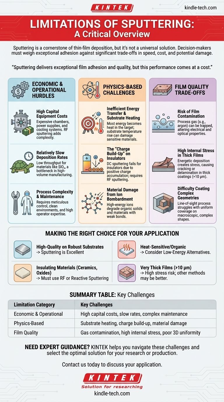
While sputtering is a cornerstone of modern thin-film deposition, it is not a universal solution. The technique is defined by a series of inherent limitations related to its cost, speed, and the aggressive nature of its physical process. These factors include high capital expenses, slow deposition rates for certain materials, significant heat generation at the substrate, and the potential for damaging sensitive materials.
Sputtering delivers exceptional film adhesion and quality, but this performance comes at a cost. Decision-makers must weigh these benefits against the significant trade-offs in process speed, equipment expense, and potential thermal or structural damage to the target and substrate.
The Economic and Operational Hurdles
Before considering the physics of the process, the practical realities of implementing sputtering present the first set of limitations. These factors often dictate whether sputtering is a viable option for a given project or production environment.
High Capital Equipment Costs
Sputtering systems are complex and expensive. The initial investment requires high-end vacuum chambers, powerful and stable power supplies, gas flow control, and often, sophisticated cooling systems.
Techniques like RF sputtering, which are necessary for depositing insulating materials, add further cost and complexity through specialized RF power generators and impedance-matching networks.
Relatively Slow Deposition Rates
Compared to other methods like thermal evaporation, sputtering can be a slow process. This is especially true for certain materials, such as oxides like silicon dioxide (SiO₂), which have a low "sputter yield."
This low throughput can be a significant bottleneck in high-volume manufacturing, increasing the cost per wafer or part.
Process Complexity and Maintenance
Achieving high-quality, pristine thin films requires meticulous process control and system maintenance. Sputtering is highly sensitive to process parameters and the cleanliness of the vacuum environment.
This necessitates regular maintenance schedules and a high degree of operator expertise to ensure reproducibility and minimize defects.
The Physics-Based Challenges
The fundamental mechanism of sputtering—ejecting atoms via high-energy ion bombardment—is the source of its most significant technical limitations.
Inefficient Energy Transfer and Substrate Heating
Most of the kinetic energy from the bombarding ions is converted into heat within the target material, not into ejecting atoms. This immense heat must be actively removed to prevent damage to the target.
A portion of this energy is also transferred to the substrate by the condensing atoms and process radiation, causing the substrate temperature to rise significantly. This can damage temperature-sensitive substrates, such as plastics or organic electronics.
The "Charge Build-Up" on Insulators
The most basic form of the technique, DC sputtering, is unsuitable for electrically insulating materials. During DC sputtering, positive ion bombardment of an insulating target leads to an accumulation of positive charge on its surface.
This charge build-up eventually repels the incoming positive argon ions, effectively extinguishing the sputtering process. This is why RF sputtering, which alternates the electrical potential, was developed.
Material Damage from Ion Bombardment
The high-energy nature of the sputtering process can be destructive. Materials with weak molecular bonds, such as organic solids, are easily degraded or decomposed by the constant ionic bombardment.
This makes sputtering a poor choice for depositing certain classes of polymers and other sensitive organic compounds without significant process modification.
Understanding the Film Quality Trade-offs
While known for producing high-quality films, sputtering presents challenges that can impact the final film's purity, stress, and uniformity, especially under specific conditions.
Risk of Film Contamination
Sputtering operates at a higher pressure (a lower vacuum) than techniques like evaporation. This means there is a higher concentration of process gas, typically argon, in the chamber.
As the film grows, these gas atoms can become incorporated or "trapped" in the film structure. This contamination can alter the film's electrical, optical, and mechanical properties.
High Internal Stress in Thick Films
The energetic arrival of sputtered atoms can create high levels of compressive or tensile stress within the growing film.
While this stress can be beneficial for adhesion in thin layers, it becomes a major problem when depositing thick coatings. High internal stress can cause the film to crack, delaminate, or peel off the substrate.
Difficulty Coating Complex Geometries
Sputtering is a line-of-sight process. While it offers excellent "step coverage" over microscopic surface features, it struggles to deposit a uniform coating on macroscopic, complex, three-dimensional shapes due to shadowing effects.
Making the Right Choice for Your Application
To determine if sputtering is appropriate, you must align its capabilities with your primary goal.
- If your primary focus is high-quality, dense films on robust substrates: Sputtering is an excellent choice, but be prepared for the high capital cost and potentially slower process times.
- If your primary focus is depositing on heat-sensitive or organic materials: The thermal load and ion bombardment from sputtering pose a significant risk; consider low-energy alternatives like thermal evaporation.
- If your primary focus is depositing insulating materials (ceramics, oxides): You must use RF or reactive sputtering, which adds cost and complexity compared to DC sputtering of metals.
- If your primary focus is producing very thick films (>10 µm): Be aware that the internal stress generated by sputtering may cause film failure; other deposition methods might be more suitable.
Ultimately, selecting the right deposition technique requires a clear understanding of your material's properties, your substrate's limitations, and your project's economic constraints.
Summary Table:
| Limitation Category | Key Challenges |
|---|---|
| Economic & Operational | High capital costs, slow deposition rates, complex maintenance |
| Physics-Based | Substrate heating, charge build-up on insulators, material damage |
| Film Quality | Risk of gas contamination, high internal stress, poor 3D coating uniformity |
Struggling to choose the right thin-film deposition technique for your specific materials and budget? The limitations of sputtering are significant, but the right lab equipment partner can help you navigate these challenges and select the optimal solution for your research or production needs. KINTEK specializes in providing high-quality lab equipment and consumables, offering expert guidance to ensure your laboratory operates at peak efficiency. Contact us today via our [#ContactForm] to discuss your application and discover how we can support your success with the right tools and expertise.
Visual Guide
Related Products
- Lab Sterile Slapping Type Homogenizer for Tissue Mashing and Dispersing
- Spark Plasma Sintering Furnace SPS Furnace
- Single Punch Manual Tablet Press Machine TDP Tablet Punching Machine
People Also Ask
- What role does a laboratory homogenizer play in radioactive cesium detection? Ensure Accuracy in Wildlife Sampling
- How does a homogenizer affect the quality of electrode slurry? Master Battery Consistency with High-Shear Mixing
- How does a laboratory automatic masticator or homogenizer facilitate the processing of biofilm samples? Optimize Accuracy
- Why is maintaining nanoparticle dispersion critical for photocatalytic reactors? Maximize Your Reaction Efficiency
- How do lab stirrers & homogenizers ensure uniform distribution? Optimize Your Complex Multiphase Chemical Mixing


