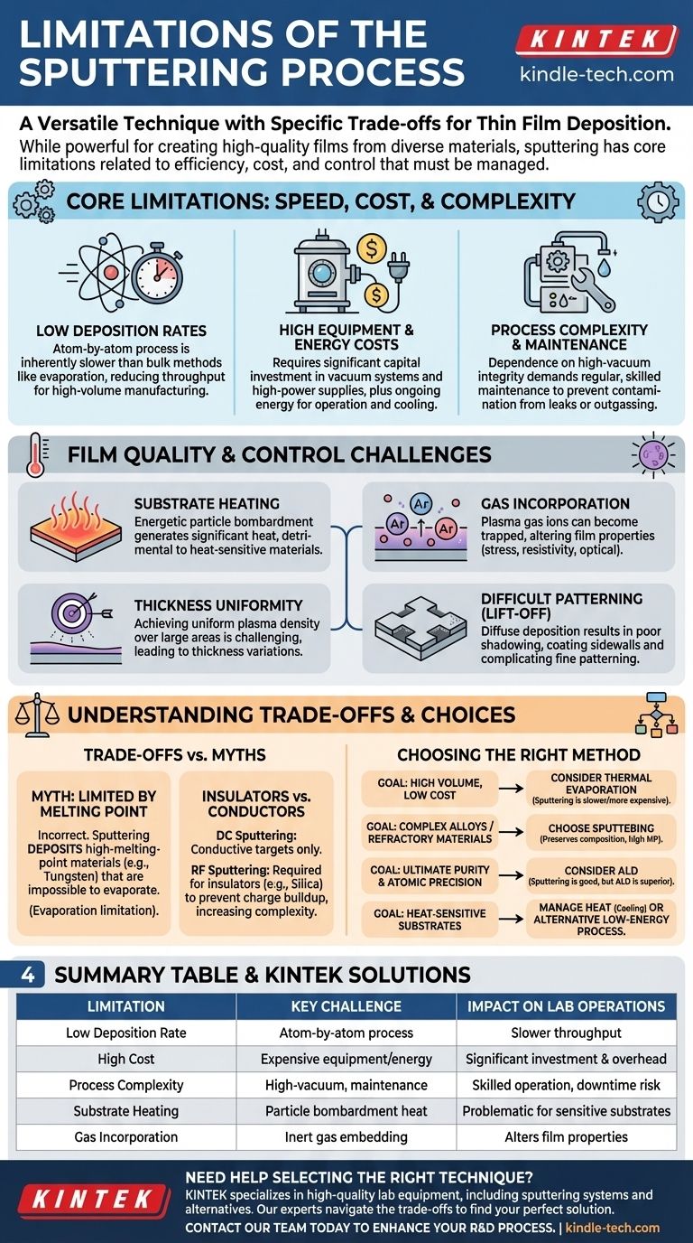
While a highly versatile deposition technique, sputtering is not without its limitations. The primary drawbacks include relatively low deposition rates, higher equipment and energy costs compared to some alternatives, and potential for film contamination from the process environment itself. The complexity of the vacuum system and power requirements also adds to its operational overhead.
Sputtering is a powerful method for creating high-quality, dense thin films from a vast range of materials. However, its main limitations are rooted in process efficiency and control—it can be slower, more expensive, and introduce specific challenges like substrate heating and gas incorporation that must be carefully managed.
Core Limitations: Speed, Cost, and Complexity
Sputtering is a physical process that relies on ejecting atoms one by one. This fundamental mechanism introduces trade-offs between quality and production efficiency.
Low Deposition Rates
Sputtering involves bombarding a target with energetic ions to physically dislodge atoms, which then deposit onto a substrate. This atom-by-atom process is inherently slower than bulk deposition methods like thermal evaporation, where material is melted and evaporates at a much higher rate.
This lower throughput can be a significant bottleneck in high-volume manufacturing environments.
High Equipment and Energy Costs
A sputtering system requires a significant capital investment. This includes a high-vacuum chamber, powerful pumps, sophisticated gas flow controllers, and high-voltage DC or radio-frequency (RF) power supplies.
The need for a cooling system to manage heat generated during the process further increases energy consumption and can reduce net production rates.
Process Complexity and Maintenance
Achieving pristine thin films requires a well-maintained, high-quality vacuum environment. Any leaks or outgassing from chamber walls can introduce impurities.
This dependency on vacuum integrity means that sputtering systems demand regular maintenance and careful operation, adding to their overall complexity.
Film Quality and Control Challenges
While known for producing dense and strongly adhered films, the sputtering process can introduce its own set of quality and control issues.
Substrate Heating
The constant bombardment of the substrate by energetic particles (including sputtered atoms and neutralized ions) generates significant heat. This can be detrimental to heat-sensitive substrates like plastics or certain semiconductor devices.
While substrate cooling can mitigate this, it adds another layer of complexity and cost to the process.
Gas Incorporation
The inert gas used to create the plasma (typically Argon) does not just strike the target. Some gas ions can become embedded within the growing film, acting as an impurity.
This incorporated gas can alter the film's mechanical stress, electrical resistivity, and optical properties.
Thickness Uniformity Over Large Areas
For large-area coatings, especially with rectangular cathodes, it can be challenging to maintain a perfectly uniform plasma density across the entire target.
This non-uniformity can lead to variations in the deposition rate, resulting in a film that is thicker in some areas and thinner in others.
Difficulty with Patterning (Lift-off)
Sputtering is a diffuse process, meaning atoms travel from the target to the substrate from many different angles. This makes it difficult to achieve the clean "shadowing" required for fine-patterning techniques like lift-off.
The poor shadowing can cause material to coat the sidewalls of the photoresist, complicating its removal and potentially contaminating the final device.
Understanding the Trade-offs
It is critical to distinguish sputtering's true limitations from those of other deposition techniques, as they are often confused.
Myth: Sputtering is Limited by Melting Point
Some sources incorrectly state that sputtering is limited by a material's melting point. This is a limitation of thermal evaporation, which requires melting the source material.
In contrast, sputtering's key advantage is its ability to deposit materials with extremely high melting points (refractory metals like tungsten or ceramics) that are impossible to evaporate practically.
Insulating vs. Conductive Materials
Basic DC sputtering only works for electrically conductive targets. If an insulating target is used, positive charge builds up on its surface, repelling the incoming ions and stopping the sputtering process.
To deposit insulators like silica or alumina, a more complex and expensive RF sputtering system is required. The rapidly oscillating electric field prevents charge accumulation, allowing the process to continue.
Precision: Sputtering vs. Atomic Layer Deposition (ALD)
While some claim sputtering offers poor thickness control, this is relative. Sputtering provides excellent and repeatable control over a film's bulk thickness, often down to the angstrom level.
However, it does not offer the perfect, self-limiting monolayer-by-monolayer growth of a technique like Atomic Layer Deposition (ALD). For applications requiring absolute atomic-level conformity and precision, ALD is superior.
Is Sputtering the Right Choice for Your Application?
Choosing a deposition method requires balancing your primary goal with the inherent limitations of the process.
- If your primary focus is high-volume, low-cost production: Sputtering's slower speed and higher cost may be a drawback; consider thermal evaporation if your material is suitable.
- If your primary focus is depositing complex alloys or refractory materials: Sputtering is a superior choice, as it effectively preserves the material's composition and is not limited by melting points.
- If your primary focus is ultimate film purity and atomic precision: Sputtering produces high-quality films, but techniques like Atomic Layer Deposition (ALD) offer a higher degree of purity and control.
- If your primary focus is coating heat-sensitive substrates: You must account for sputtering's inherent substrate heating and implement robust cooling or choose a lower-energy process.
By understanding these specific limitations, you can leverage sputtering's unique strengths for applications where film density, adhesion, and material versatility are paramount.
Summary Table:
| Limitation | Key Challenge | Impact on Lab Operations |
|---|---|---|
| Low Deposition Rate | Atom-by-atom process is inherently slow | Slower throughput for high-volume manufacturing |
| High Cost | Expensive equipment and high energy consumption | Significant capital investment and operational overhead |
| Process Complexity | Requires high-vacuum environment and regular maintenance | Demands skilled operation and increases downtime risk |
| Substrate Heating | Energetic particle bombardment generates heat | Problematic for heat-sensitive substrates like plastics |
| Gas Incorporation | Inert plasma gas can embed in the film | Can alter film's electrical and mechanical properties |
Need help selecting the right thin film deposition technique for your specific materials and application?
At KINTEK, we specialize in providing high-quality lab equipment, including sputtering systems and alternatives like thermal evaporators. Our experts can help you navigate the trade-offs between speed, cost, and film quality to find the perfect solution for your laboratory's unique needs.
Contact our team today to discuss your project and discover how KINTEK's solutions can enhance your research and development process.
Visual Guide