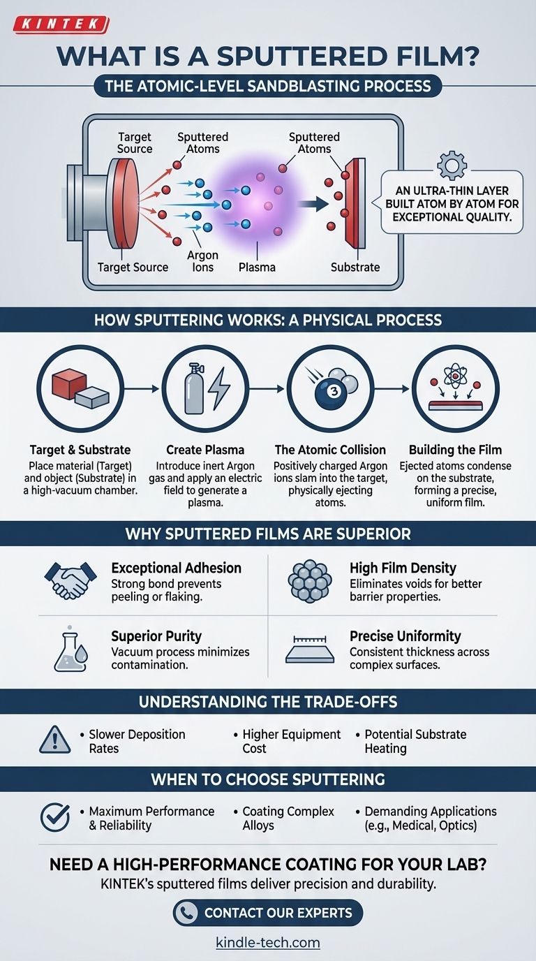
In short, a sputtered film is an ultra-thin layer of material deposited onto a surface using a process called sputtering. This technique physically knocks atoms off a source material (the "target") and onto the desired object (the "substrate") within a vacuum, essentially building the film one atom at a time. This method is renowned for creating coatings with exceptional quality and performance.
Sputtering is best understood as a highly controlled, atomic-level sandblasting process. Instead of melting a material and letting it condense, sputtering uses energetic ions to precisely eject atoms, resulting in films with superior density, adhesion, and purity.
How Sputtering Works: A Physical Process
Unlike painting or plating, sputtering is a Physical Vapor Deposition (PVD) technique. It doesn't rely on chemical reactions or high heat to melt the source material. Instead, it uses momentum.
The Target and Substrate
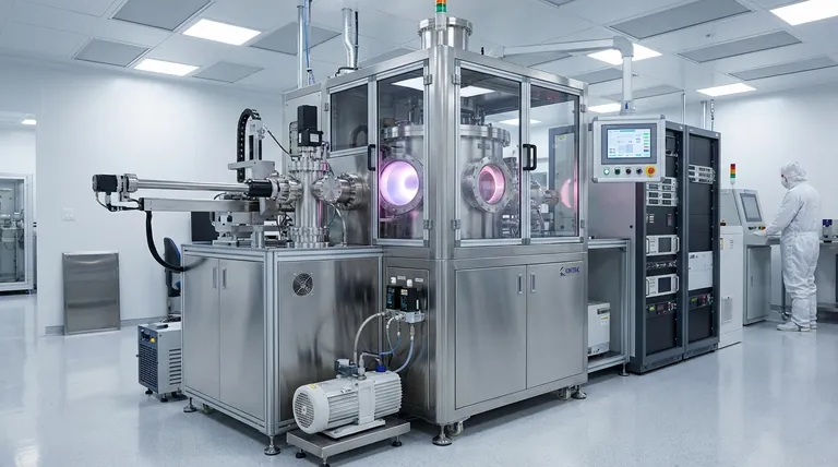
The process begins with two key items inside a vacuum chamber: the target and the substrate. The target is a piece of the material you want to create a film of (e.g., titanium, gold, or a ceramic). The substrate is the object you want to coat.
Creating a Plasma
The chamber is pumped down to a high vacuum to remove contaminants. A small amount of an inert gas, typically Argon, is then introduced. An electric field is applied, which strips electrons from the Argon atoms, creating a glowing, ionized gas called a plasma.
The Atomic "Billiard Shot"
The positively charged Argon ions in the plasma are accelerated by the electric field and slam into the negatively charged target. This high-energy collision is like a powerful billiard break shot at the atomic level.
The impact has enough momentum to physically knock atoms loose from the target material. These ejected atoms are now "sputtered."
Building the Film
These sputtered atoms travel through the vacuum and land on the substrate, condensing to form a thin, highly uniform film. Because this process is so controlled, the film's thickness can be managed with incredible precision, often down to the single-nanometer level.
Why Sputtered Films Are Superior
The physical nature of the sputtering process is directly responsible for the high-quality characteristics mentioned in technical specifications. The benefits are not incidental; they are a direct result of the physics involved.
Exceptional Density and Adhesion
Sputtered atoms arrive at the substrate with significant kinetic energy. This energy helps them pack together very tightly, eliminating voids and creating a highly dense film. This energy also helps the atoms embed slightly into the substrate's surface, resulting in excellent adhesion that is far stronger than many other coating methods.
Unmatched Purity
The entire process occurs in a high vacuum, which minimizes the chance for atmospheric gases like oxygen or water vapor to become trapped in the film. Furthermore, since the target material isn't melted in a container (a crucible), there are no impurities introduced from a secondary source.
Precise Uniformity
Sputtering allows for extremely fine control over the deposition rate. By managing the gas pressure and electrical power, films can be grown with exceptional thickness uniformity across the entire surface of the substrate, which is critical for applications like semiconductors and optical lenses.
Understanding the Trade-offs
No process is perfect for every application. Objectivity requires acknowledging where sputtering may not be the ideal choice.
Slower Deposition Rates
Sputtering is a very deliberate, atom-by-atom process. Consequently, its deposition rates are often significantly lower than other methods like thermal evaporation. For applications requiring very thick coatings quickly, sputtering can be inefficient.
Equipment Complexity and Cost
Sputtering systems require sophisticated and expensive equipment, including high-vacuum chambers, specialized power supplies, and gas handling systems. This makes the initial investment and operational costs higher than simpler coating techniques.
Potential Substrate Heating
The high-energy ion bombardment and condensing atoms can transfer a significant amount of heat to the substrate. While this can improve film properties, it can also damage heat-sensitive substrates like plastics or certain electronic components.
When to Choose Sputtering
Your choice of deposition method should always align with your end goal and the performance requirements of your product.
- If your primary focus is maximum performance and reliability: Sputtering is the definitive choice for applications like semiconductor manufacturing, medical implants, and high-performance optics where film purity, density, and adhesion are non-negotiable.
- If your primary focus is coating complex alloys: Sputtering excels at depositing films from alloy or compound targets because the process tends to preserve the original material's chemical composition (stoichiometry).
- If your primary focus is rapid, low-cost production: For less demanding applications like decorative coatings on consumer goods, simpler methods like thermal evaporation may provide a more cost-effective solution.
Ultimately, choosing sputtering is an investment in the precision, durability, and fundamental quality of your material's surface.
Summary Table:
| Key Characteristic | Why It Matters |
|---|---|
| Exceptional Adhesion | Strong bond to the substrate prevents peeling or flaking. |
| High Film Density | Eliminates voids for better barrier properties and durability. |
| Superior Purity | Vacuum process minimizes contamination for critical applications. |
| Precise Uniformity | Consistent thickness across complex surfaces for reliable performance. |
Need a high-performance coating for your lab equipment or consumables?
Sputtered films from KINTEK deliver the precision, purity, and durability required for demanding laboratory applications. Our expertise in PVD technology ensures your substrates—from sensor components to specialized labware—receive a coating that enhances performance and longevity.
Contact our thin-film experts today to discuss how sputtering can solve your specific coating challenge.
Visual Guide
Related Products
- Lab Blown Film Extrusion Three Layer Co-Extrusion Film Blowing Machine
- Tungsten Evaporation Boat for Thin Film Deposition
- Aluminum-Plastic Flexible Packaging Film for Lithium Battery Packaging
People Also Ask
- What is the use of a blown film machine? To Produce Strong, Versatile Plastic Films for Packaging
- What is the blown film technique? A Guide to High-Strength Plastic Film Production
- What does a blown film machine do? Transform Plastic Pellets into Versatile Film
- What is the blown film extrusion method? Master the Art of Strong, Seamless Plastic Film Production
- What is the cost of blown film extrusion? From $20K to High-End Systems


