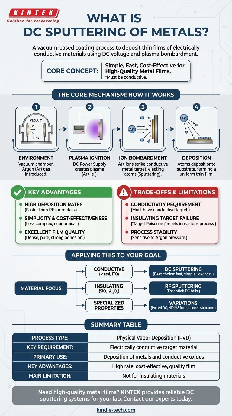
At its core, DC sputtering is a vacuum-based coating process used to deposit thin films of electrically conductive materials. It operates by creating a plasma and using a direct current (DC) voltage to bombard a source material, known as the "target," with ions. This bombardment physically ejects atoms from the target, which then travel and deposit onto a "substrate," forming a uniform, high-purity thin film.
The central concept to grasp is that DC sputtering is a simple, fast, and cost-effective method for depositing high-quality metal films. Its primary and most critical limitation is that it only works for materials that can conduct electricity.
The Core Mechanism: How DC Sputtering Works
To understand why DC sputtering is so widely used for metals, it's essential to visualize the step-by-step physical process happening inside the vacuum chamber.
Step 1: Creating the Environment
The process begins by placing the source material (target) and the object to be coated (substrate) into a vacuum chamber. The chamber is pumped down to a very low pressure to remove contaminants.
A small amount of an inert gas, almost always Argon (Ar), is then introduced into the chamber.
Step 2: Igniting the Plasma
A high-voltage direct current (DC) power supply is connected, applying a large negative charge to the metal target. The chamber walls or a separate anode are held at ground potential (positive relative to the target).
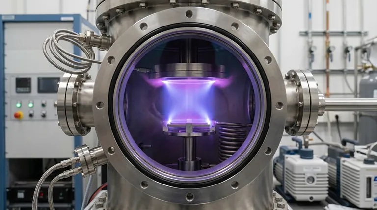
This strong electric field energizes the argon gas, stripping electrons from the argon atoms and creating a mixture of positive argon ions (Ar+) and free electrons. This ionized gas is known as a plasma, which often glows purple or blue.
Step 3: Ion Bombardment and Ejection
The positively charged argon ions (Ar+) are powerfully accelerated by the electric field towards the negatively charged metal target.
These high-energy ions collide with the target surface with significant force. The impact transfers momentum to the target atoms, knocking them loose and ejecting them from the surface. This ejection process is the "sputtering."
Step 4: Deposition and Film Growth
The sputtered atoms from the target travel in straight lines through the low-pressure chamber until they strike the substrate.
Upon arrival, these atoms condense on the substrate's surface, gradually building up, layer by layer, to form a dense and highly uniform thin film.
Key Advantages for Metal Deposition
DC sputtering is not just one option for metals; for many applications, it is the preferred method due to its distinct advantages.
High Deposition Rates
For most metals, DC sputtering is significantly faster than alternative techniques like RF (Radio Frequency) sputtering. This high throughput makes it ideal for industrial-scale production.
Simplicity and Cost-Effectiveness
The power supply and equipment needed for a DC system are less complex and therefore less expensive than those required for RF systems. This makes it an accessible and economical choice.
Excellent Film Quality
The process produces films that are very dense, pure, and have strong adhesion to the substrate. The thickness of the film can be precisely controlled by adjusting parameters like power, time, and gas pressure.
Understanding the Trade-offs and Limitations
No technique is perfect. The strengths of DC sputtering are directly tied to its critical limitation.
The Conductivity Requirement
This is the most important takeaway. The DC voltage requires a conductive path to function. The target must be able to conduct electricity to maintain its negative charge and dissipate the positive charge delivered by the arriving ions.
Insulating Target Failure
If you attempt to use DC sputtering on an insulating material (like a ceramic or an oxide), positive charge from the argon ions immediately builds up on the target surface. This effect, known as "target poisoning," repels subsequent positive ions, effectively shutting down the sputtering process.
Process Stability
While robust, the process is sensitive to the argon gas pressure. Too high a pressure can lead to excessive gas scattering and lower film quality, while too low a pressure can make it difficult to sustain the plasma.
How to Apply This to Your Goal
Your choice of sputtering technique is determined entirely by the material you need to deposit.
- If your primary focus is depositing a conductive metal or transparent conductive oxide (like ITO): DC sputtering is almost always the correct choice due to its speed, simplicity, and low cost.
- If your primary focus is depositing an insulating material (like SiO₂, Al₂O₃, or TiN): You must use RF sputtering, as a DC voltage cannot be sustained on a non-conductive target.
- If your primary focus is achieving specialized film properties for advanced applications: You may need to explore variations like pulsed DC sputtering or High-Power Impulse Magnetron Sputtering (HiPIMS) for enhanced film density and structure control.
By understanding this fundamental distinction, you can confidently select the most effective deposition technology for your specific material and application.
Summary Table:
| Feature | Description |
|---|---|
| Process Type | Physical Vapor Deposition (PVD) |
| Key Requirement | Target material must be electrically conductive |
| Primary Use | Deposition of metals and conductive oxides |
| Key Advantages | High deposition rates, cost-effectiveness, excellent film quality |
| Main Limitation | Cannot be used on insulating materials |
Need to deposit a high-quality metal film? KINTEK specializes in lab equipment and consumables, providing reliable DC sputtering systems for your laboratory needs. Our solutions deliver the speed, simplicity, and excellent film quality you require for conductive coatings. Contact our experts today to discuss how we can support your specific application and enhance your lab's capabilities!
Visual Guide
Related Products
- Spark Plasma Sintering Furnace SPS Furnace
- Vacuum Induction Melting Spinning System Arc Melting Furnace
- Circulating Water Vacuum Pump for Laboratory and Industrial Use
People Also Ask
- What is the theory of spark plasma sintering? A Guide to Rapid, Low-Temperature Densification
- What is SPS sintering method? A Guide to High-Speed, High-Performance Material Fabrication
- What are the fundamentals of spark plasma sintering process? Unlock Rapid, High-Performance Material Consolidation
- What is the process fundamentals of spark plasma sintering? Achieve Rapid, High-Density Material Consolidation
- What is the difference between spark plasma sintering and flash sintering? A Guide to Advanced Sintering Methods


