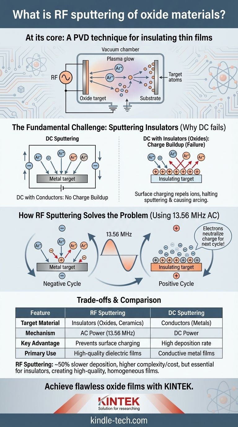
At its core, RF sputtering is a physical vapor deposition (PVD) technique used to deposit thin films of electrically insulating materials, such as oxides, onto a substrate. It solves a fundamental problem that simpler methods cannot by using a high-frequency alternating current to prevent a fatal charge buildup on the insulating target material, which allows for a continuous and stable deposition process.
While direct current (DC) sputtering works for metals, it fails with insulating materials like oxides due to electrostatic charge buildup. RF sputtering overcomes this by using a rapidly alternating electric field to continuously neutralize the target surface, enabling the consistent deposition of high-quality dielectric films critical for modern optics and semiconductors.
The Fundamental Challenge: Sputtering Insulators
To understand RF sputtering, you must first understand why the more straightforward DC sputtering method is unsuitable for materials like oxides, nitrides, or ceramics.
Why DC Sputtering Fails with Oxides
In any sputtering process, a target material is bombarded by positive ions (typically Argon) from a plasma. This impact physically ejects, or "sputters," atoms from the target, which then travel and coat a nearby substrate.
In DC sputtering, a constant negative voltage is applied to the target to attract these positive ions. If the target is a conductor (like a metal), it can easily dissipate the positive charge from the arriving ions.
However, if the target is an insulator like an oxide, the positive charge from the ions accumulates on its surface.
The Consequence of Surface Charging
This buildup of positive charge on the insulating target surface, known as surface charging, has a catastrophic effect. It begins to electrostatically repel the incoming positive Argon ions.
Eventually, this repulsion becomes so strong that it stops the bombardment entirely, halting the sputtering process. This can also lead to uncontrolled arcing in the plasma, damaging the substrate and compromising film quality.
How RF Sputtering Solves the Problem
RF sputtering circumvents the surface charging issue by replacing the constant DC voltage with a high-frequency alternating current (AC) power source, almost universally set at 13.56 MHz.
The Role of the Alternating Field
This radio frequency field rapidly alternates the voltage on the target, switching it between negative and positive potential millions of times per second. This creates a two-part cycle that allows for continuous sputtering of insulators.
The Negative Cycle: Sputtering the Target
During the half-cycle when the target is negatively biased, it functions just like a DC target. It attracts the heavy, positive Argon ions, which bombard the surface and sputter material away toward the substrate. During this time, a cloud of highly mobile electrons from the plasma is repelled from the target.
The Positive Cycle: Neutralizing the Surface
During the brief half-cycle when the target becomes positively biased, the process reverses. The positive target now attracts the massive cloud of mobile electrons that were previously repelled.
This flood of electrons effectively neutralizes the positive charge that built up on the target surface during the sputtering phase. Think of it as wiping a whiteboard clean before you write on it again, ensuring there's no leftover charge to interfere with the next sputtering cycle.
Understanding the Trade-offs
While RF sputtering is a powerful solution, its mechanism introduces specific trade-offs compared to the simpler DC method.
Lower Deposition Rate
The RF process is inherently less efficient. Because a portion of each cycle is dedicated to neutralizing the target rather than sputtering it, the effective power delivered for deposition is lower. As a general rule, the deposition rate of RF sputtering is about 50% that of DC sputtering for a given power input.
Higher System Complexity and Cost
RF systems require more sophisticated equipment, including an RF power supply and an impedance matching network to efficiently transfer power into the plasma. This makes RF sputtering systems more complex and expensive to build and maintain than their DC counterparts.
Suitability for Specific Applications
Due to the lower deposition rates and higher costs, RF sputtering is typically reserved for applications where depositing an insulating material is essential. It is widely used for creating high-quality, homogeneous films at low substrate temperatures, which is critical for sensitive electronics and precision optics.
Making the Right Choice for Your Goal
Selecting the correct sputtering technique is a strategic decision based entirely on the electrical properties of your target material and your production goals.
- If your primary focus is depositing a conductive film (e.g., a metal): Use DC sputtering for its higher deposition rate, lower cost, and simpler operation.
- If your primary focus is depositing a high-quality insulating film (e.g., an oxide, nitride, or ceramic): RF sputtering is the necessary and correct choice, as DC sputtering is not viable.
- If your primary focus is high-throughput production at the lowest cost: DC sputtering is strongly preferred, but this is only an option for conductive materials.
Ultimately, choosing RF sputtering is a non-negotiable requirement when your work depends on creating precise thin films from electrically insulating materials.
Summary Table:
| Feature | RF Sputtering | DC Sputtering |
|---|---|---|
| Target Material | Insulators (Oxides, Ceramics) | Conductors (Metals) |
| Mechanism | AC Power (13.56 MHz) | DC Power |
| Key Advantage | Prevents surface charging | High deposition rate |
| Primary Use | High-quality dielectric films | Conductive metal films |
Need to deposit a flawless oxide film? RF sputtering is the key to achieving uniform, high-quality coatings for your most demanding applications in semiconductors, optics, and research. KINTEK specializes in advanced lab equipment, including sputtering systems, to meet your precise laboratory needs. Contact our experts today to discuss how we can provide the right solution for your thin film deposition challenges.
Visual Guide
Related Products
- RF PECVD System Radio Frequency Plasma-Enhanced Chemical Vapor Deposition RF PECVD
- Spark Plasma Sintering Furnace SPS Furnace
- Horizontal High Temperature Graphite Vacuum Graphitization Furnace
People Also Ask
- What is the role of RF-PECVD in VFG preparation? Mastering Vertical Growth and Surface Functionality
- What is plasma enhanced chemical vapour deposition PECVD used for? Enable Low-Temp Thin Films for Electronics & Solar
- What is plasma chemical vapor deposition? A Low-Temperature Thin Film Coating Solution
- How does Radio Frequency Enhanced Plasma Chemical Vapour Deposition (RF-PECVD) work? Learn the Core Principles
- What is plasma enhanced chemical vapour deposition process? Unlock Low-Temperature, High-Quality Thin Films


