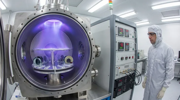
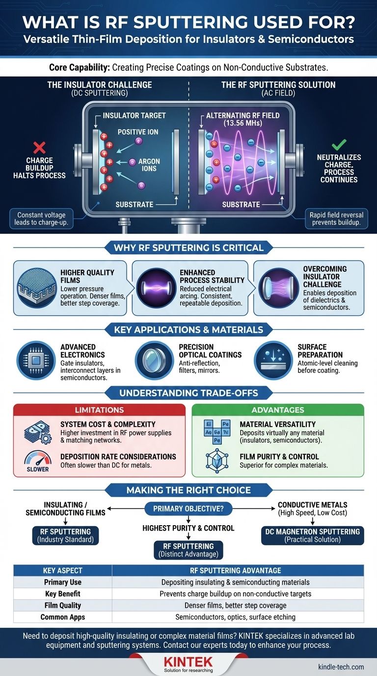
At its core, RF sputtering is a highly versatile thin-film deposition technique used for creating precise coatings on a substrate. Its most critical capability, however, is the ability to deposit materials that are electrical insulators or semiconductors. This makes it indispensable for manufacturing advanced electronics, optical devices, and other high-technology components where other methods like DC sputtering would fail.
The fundamental challenge with sputtering insulating materials is electrical charge buildup, which quickly halts the process. RF sputtering solves this by using an alternating radio-frequency field, making it the go-to method for depositing the dielectric and semiconducting layers essential for modern microchips and precision optics.
Why RF Sputtering is a Critical Deposition Tool
The primary advantage of RF sputtering stems from its use of an alternating current (AC) power source, typically at a radio frequency of 13.56 MHz. This fundamental difference from direct current (DC) sputtering unlocks unique capabilities.
Overcoming the Insulator Challenge
In DC sputtering, a constant negative voltage is applied to the target material. This works perfectly for conductive targets, but if the target is an insulator, positive ions build up on its surface.
This charge buildup, or "charge-up," creates an opposing electric field that repels the incoming ions, quickly extinguishing the sputtering process.
The rapid reversal of the electric field in RF sputtering prevents this. During one half of the cycle, the target is bombarded by ions, and during the other half, it is flooded with electrons, neutralizing any accumulated positive charge and allowing the process to continue indefinitely.
Achieving Higher Quality Films
RF sputtering can sustain a stable plasma at lower operating pressures than standard DC sputtering.
Operating in a higher vacuum means there are fewer gas molecules for the sputtered atoms to collide with on their way to the substrate. This results in a more direct path, leading to denser films and better step coverage over complex surface topographies.
The oscillating electrons in the RF plasma also ionize the sputtering gas more efficiently, leading to higher deposition rates compared to DC sputtering at the same low pressure.
Enhancing Process Stability
The alternating field used in RF sputtering significantly reduces the electrical arcing that can be problematic in other processes.
This leads to a more stable and repeatable deposition, which is critical for manufacturing processes with tight tolerances. It also avoids issues like the "disappearing anode," ensuring consistent performance over long periods.
Key Applications and Material Capabilities
The ability to deposit virtually any material makes RF sputtering a cornerstone technology in several advanced industries.
Manufacturing Advanced Electronics
RF sputtering is essential in the semiconductor industry. It is used to deposit the thin dielectric films that form critical components like gate insulators in transistors and insulating layers between metal interconnects.
Creating Precision Optical Coatings
The technique is widely used to create complex optical filters, anti-reflection coatings on lenses, and reflective coatings for mirrors. The precise control over the thickness and composition of dielectric layers is a key advantage here.
Sputtering for Surface Preparation
Beyond deposition, the sputtering process itself is a highly effective cleaning method. By briefly using a substrate as the target, surface contaminants can be etched away at an atomic level to prepare an ultra-pure surface before a coating is applied.
Understanding the Trade-offs and Limitations
While powerful, RF sputtering is not always the ideal choice. Objectivity requires acknowledging its specific disadvantages.
System Cost and Complexity
The primary drawback of RF sputtering is cost. RF power supplies and their required impedance matching networks are significantly more expensive and complex than their DC counterparts.
This higher initial investment can make it less economical for applications where simpler methods suffice.
Deposition Rate Considerations
While RF sputtering is highly efficient at low pressures, DC magnetron sputtering can often achieve higher deposition rates for conductive metal targets. The choice often depends on whether film quality or raw throughput is the priority.
Substrate Size Limitations
Historically, RF sputtering systems have often been engineered for smaller substrate sizes, such as those found in research and development or specialized semiconductor manufacturing. Scaling the technology for very large area applications can present additional challenges.
Making the Right Choice for Your Goal
Selecting the correct deposition method depends entirely on the material you are working with and your primary objective.
- If your primary focus is depositing insulating or semiconducting films: RF sputtering is the necessary and standard industry choice.
- If your primary focus is depositing conductive metals at high speed and low cost: DC magnetron sputtering is often the more practical and economical solution.
- If your primary focus is achieving the highest possible film purity and process control for a complex material: RF sputtering's stable, low-pressure operation provides a distinct advantage.
Ultimately, understanding the unique capabilities of RF sputtering allows you to select the precise tool needed to engineer materials at the atomic scale.
Summary Table:
| Key Aspect | RF Sputtering Advantage |
|---|---|
| Primary Use | Depositing insulating (dielectric) and semiconducting materials |
| Key Benefit | Prevents charge buildup on non-conductive targets |
| Film Quality | Denser films, better step coverage due to low-pressure operation |
| Common Applications | Semiconductor manufacturing, precision optical coatings, surface etching |
| Main Limitation | Higher system cost and complexity compared to DC sputtering |
Need to deposit high-quality insulating or complex material films?
KINTEK specializes in advanced lab equipment, including sputtering systems tailored for R&D and production. Our expertise can help you select the right deposition technology to achieve superior film quality, process stability, and precise control for your specific materials—whether for semiconductor, optical, or other advanced applications.
Contact our experts today to discuss how our solutions can enhance your thin-film deposition process.
Visual Guide
Related Products
- RF PECVD System Radio Frequency Plasma-Enhanced Chemical Vapor Deposition RF PECVD
- Spark Plasma Sintering Furnace SPS Furnace
- Horizontal High Temperature Graphite Vacuum Graphitization Furnace
People Also Ask
- What is plasma enhanced chemical Vapour deposition process used for fabrication of? A Guide to Low-Temperature Thin Films
- What is an example of PECVD? RF-PECVD for High-Quality Thin Film Deposition
- What is plasma enhanced chemical vapour deposition process? Unlock Low-Temperature, High-Quality Thin Films
- How does Radio Frequency Enhanced Plasma Chemical Vapour Deposition (RF-PECVD) work? Learn the Core Principles
- What is plasma CVD? Unlock Low-Temperature Thin Film Deposition for Sensitive Materials


