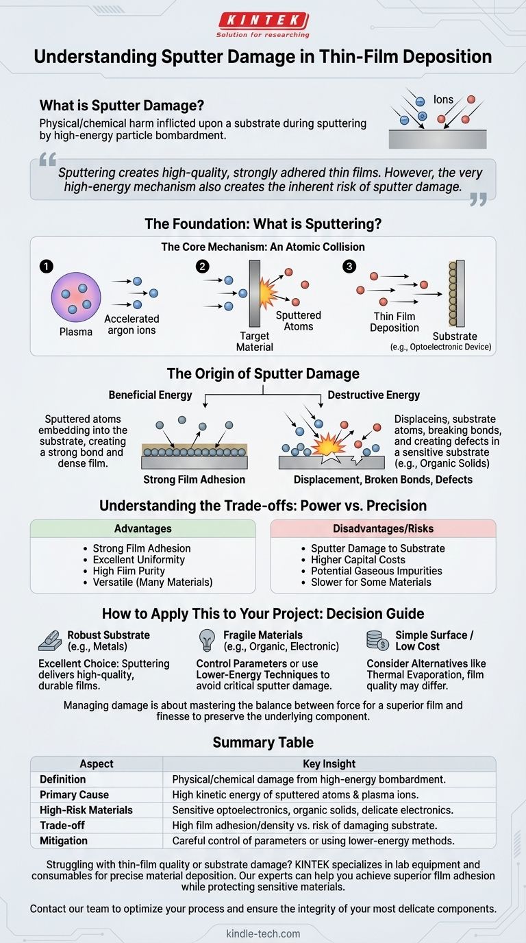
In the world of advanced material science, sputter damage refers to the physical or chemical harm inflicted upon a substrate during the thin-film deposition process known as sputtering. This damage is caused by the bombardment of the substrate by highly energetic particles, a common concern when depositing materials like transparent electrodes onto sensitive optoelectronic devices.
Sputtering is a powerful and versatile method for creating high-quality, strongly adhered thin films. However, the very high-energy mechanism that makes it so effective is also its primary drawback, creating the inherent risk of sputter damage to the underlying material.
What is Sputtering? The Foundation of the Process
To understand the damage, you must first understand the process. Sputtering is a physical vapor deposition (PVD) technique used to create exceptionally thin and uniform films on a variety of surfaces.
The Core Mechanism: An Atomic Collision
The process begins by creating a plasma and accelerating ions from an inert gas (like argon) toward a source material, known as the target.
When these high-energy ions strike the target, they transfer their momentum, knocking out or "sputtering" atoms from the target material.
These ejected atoms then travel through the vacuum chamber and deposit onto the substrate, gradually building up a thin film with excellent properties.
The Origin of Sputter Damage
The same energy that makes sputtering so effective at creating dense, well-adhered films is also the source of potential damage.
The Role of High-Energy Particles
The sputtered atoms leave the target with significant kinetic energy. This energy is beneficial, as it helps the atoms embed slightly into the substrate surface, creating a very strong bond and a dense film structure.
When Energy Becomes Destructive
If the substrate is sensitive, this high-energy bombardment can be destructive. It can displace atoms in the substrate's crystal lattice, break chemical bonds, or alter the material's electronic properties.
This is particularly true for materials like organic solids, which can easily degrade under ionic bombardment. For delicate electronic components, this can introduce defects that impair or destroy device function.
Understanding the Trade-offs: Power vs. Precision
Choosing sputtering is a decision based on a clear set of advantages that must be weighed against its inherent risks, including sputter damage.
The Advantages of Sputtering
Sputtering is widely used in mass production for good reason. It offers strong film adhesion and excellent uniformity over large areas.
The process provides high film purity and density with few defects like pinholes. Critically, it can be used to deposit virtually any material, including compounds and elements with extremely high melting points that are difficult to handle with other methods.
The Disadvantages and Risks
The primary technical risk is sputter damage to the substrate. The process can also be slower than alternatives for certain materials and tends to have higher capital equipment costs.
Furthermore, because it operates in a lesser vacuum range than techniques like evaporation, there can be a greater tendency to introduce gaseous impurities into the film or substrate.
How to Apply This to Your Project
Your choice of deposition method must align with your material's sensitivity and your final goal for film quality.
- If your primary focus is film adhesion and density on a robust substrate: Sputtering is an excellent choice due to the high-quality, durable films it produces.
- If your primary focus is depositing on fragile organic or electronic materials: You must carefully control sputtering parameters (e.g., pressure, power) or consider lower-energy techniques to avoid critical sputter damage.
- If your primary focus is coating a simple, non-sensitive surface at lower cost: A process like thermal evaporation might be sufficient, though the resulting film quality may not match that of a sputtered film.
Ultimately, managing sputter damage is about mastering the balance between the force needed for a superior film and the finesse required to preserve your underlying component.
Summary Table:
| Aspect | Key Insight |
|---|---|
| Definition | Physical/chemical damage to a substrate caused by high-energy particle bombardment during sputtering. |
| Primary Cause | The high kinetic energy of sputtered atoms and plasma ions used in the deposition process. |
| High-Risk Materials | Sensitive optoelectronic devices, organic solids, and delicate electronic components. |
| Trade-off | High film adhesion and density vs. the risk of damaging the underlying substrate. |
| Mitigation | Careful control of sputtering parameters (pressure, power) or using lower-energy deposition techniques. |
Struggling with thin-film quality or substrate damage? KINTEK specializes in lab equipment and consumables for precise material deposition. Our experts can help you select the right sputtering system or alternative method to achieve superior film adhesion while protecting your sensitive materials. Contact our team today to optimize your process and ensure the integrity of your most delicate components.
Visual Guide
Related Products
- Chemical Vapor Deposition CVD Equipment System Chamber Slide PECVD Tube Furnace with Liquid Gasifier PECVD Machine
- Vacuum Induction Melting Spinning System Arc Melting Furnace
- Spark Plasma Sintering Furnace SPS Furnace
- Split Chamber CVD Tube Furnace with Vacuum Station Chemical Vapor Deposition System Equipment Machine
- Multi Heating Zones CVD Tube Furnace Machine Chemical Vapor Deposition Chamber System Equipment
People Also Ask
- What are the core advantages of PE-CVD in OLED encapsulation? Protect Sensitive Layers with Low-Temp Film Deposition
- What are the processes of vapor phase deposition? Understand CVD vs. PVD for Superior Thin Films
- What types of substrates are used in CVD to facilitate graphene films? Optimize Graphene Growth with the Right Catalyst
- Why is Chemical Vapor Deposition (CVD) equipment uniquely suited for constructing hierarchical superhydrophobic structures?
- How are carbon nanotubes grown? Master Scalable Production with Chemical Vapor Deposition