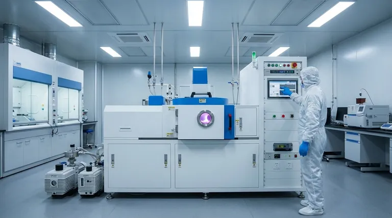
In essence, sputtering is a physical deposition process used to create exceptionally thin and uniform films of material. Unlike methods that melt a source material, sputtering physically knocks atoms off a solid "target" using high-energy ion bombardment inside a vacuum. These ejected atoms then travel and deposit onto a component, building the desired coating one atom at a time.
Sputtering is best understood not as a melting process, but as a microscopic game of "atomic billiards." It uses momentum from energized gas ions to precisely chip away at a source material, providing a controlled way to build high-quality films with excellent adhesion and purity.
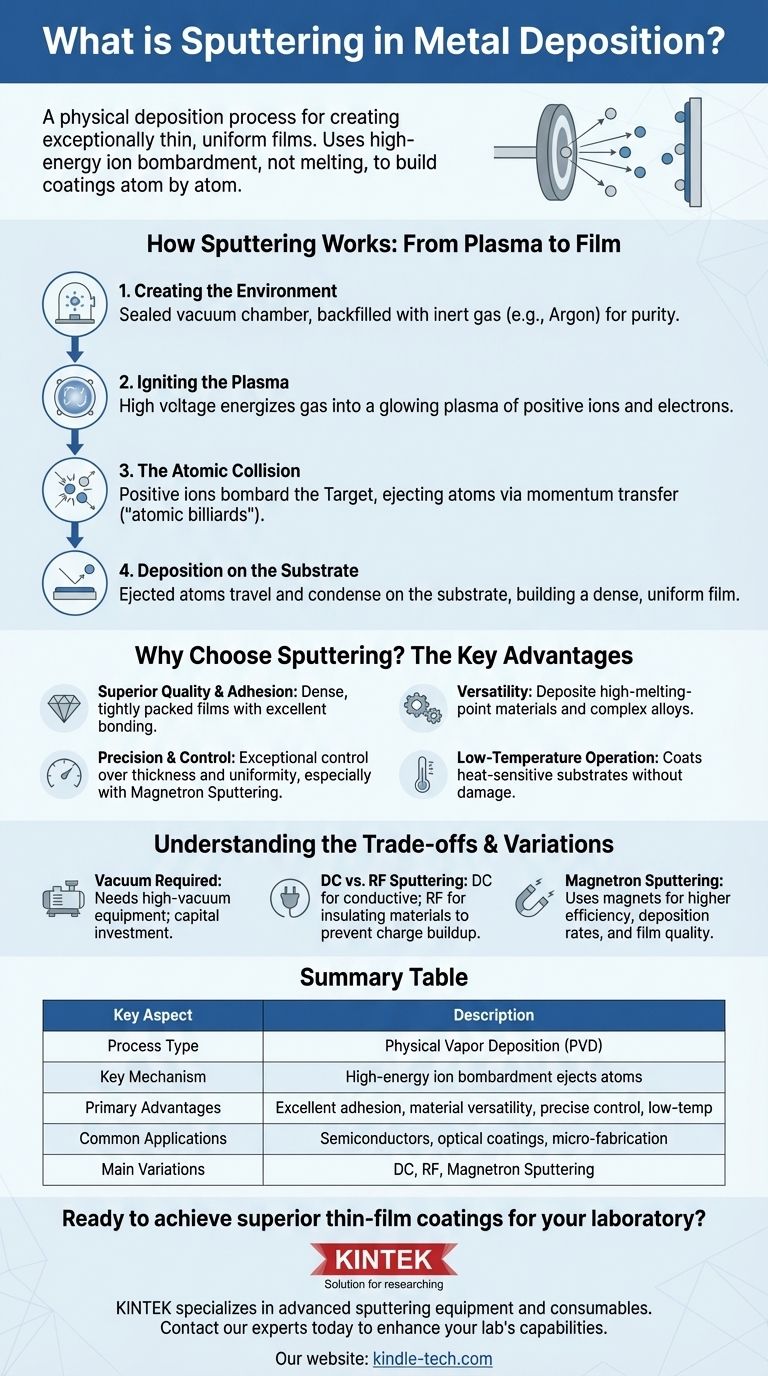
How Sputtering Works: From Plasma to Film
Sputter deposition is a type of Physical Vapor Deposition (PVD) that relies on a well-controlled sequence of physical events rather than chemical reactions or thermal evaporation.
Step 1: Creating the Environment
The entire process takes place inside a sealed vacuum chamber. This chamber is first evacuated and then backfilled with a small, controlled amount of an inert gas, most commonly Argon (Ar).
This inert gas is critical because it will not chemically react with the target material or the substrate, ensuring the purity of the final film.
Step 2: Igniting the Plasma
A high voltage is applied within the chamber, which energizes the inert gas and transforms it into a plasma.
A plasma is a state of matter where gas atoms are broken into positive ions and free electrons, creating an energized, glowing cloud.
Step 3: The Atomic Collision
The positively charged gas ions from the plasma are accelerated by an electric field and slam into the surface of the target, which is the source material for the coating.
If the energy of these bombarding ions is high enough, they transfer their momentum to the target atoms, knocking them loose and ejecting them into the vacuum chamber. This ejection of atoms is the "sputtering" effect.
Step 4: Deposition on the Substrate
The freed atoms from the target travel through the vacuum chamber until they strike the surface of the part being coated, known as the substrate.
Upon impact, these atoms stick and condense, gradually building up a thin, dense, and highly uniform film. A shutter is often used to precisely control the start and stop of the deposition.
Why Choose Sputtering? The Key Advantages
Sputtering is a dominant technique in many high-tech industries because of the unique qualities of the films it produces.
Superior Film Quality and Adhesion
Because the sputtered atoms arrive at the substrate with significant energy, they form a very dense and tightly packed film. This results in coatings with extremely strong adhesion to the substrate.
Versatility with Materials
Sputtering does not rely on melting the source material. This makes it ideal for depositing materials with extremely high melting points, such as carbon or silicon, as well as complex alloys whose composition must be preserved.
Precision and Control
Modern sputtering systems, particularly magnetron sputtering, offer exceptional control over film thickness, uniformity, and composition. This precision is critical for optical coatings, semiconductors, and other micro-fabrication processes.
Low-Temperature Operation
The sputtering process can be conducted at relatively low temperatures. This allows for the coating of heat-sensitive substrates, such as plastics, without causing damage.
Understanding the Trade-offs and Variations
While powerful, sputtering is a complex process with specific requirements and variations suited for different applications.
The Need for a Vacuum
Sputtering requires high-vacuum equipment, which is a significant capital investment. The process cannot be performed in a standard atmospheric environment.
DC vs. RF Sputtering
The type of power source used defines the capability of the system. Direct Current (DC) sputtering is effective for electrically conductive target materials. For insulating materials, a Radio Frequency (RF) source is required to prevent charge buildup on the target surface that would otherwise halt the process.
The Role of Magnetron Sputtering
Magnetron sputtering is an advanced form of the technique that uses powerful magnets behind the target. These magnets trap electrons near the target's surface, dramatically increasing the efficiency of the gas ionization. This leads to much higher deposition rates and better film quality, making it the standard for most industrial applications.
When is Sputtering the Right Choice?
Choosing the right deposition technique depends entirely on the required properties of the final film and the material being used.
- If your primary focus is high-purity films and strong adhesion: Sputtering excels at creating dense, well-bonded coatings that are difficult to achieve with other methods.
- If your primary focus is depositing complex alloys or high-melting-point materials: Sputtering's non-thermal nature preserves the material's original composition perfectly.
- If your primary focus is coating large, flat surfaces with extreme uniformity: Magnetron sputtering is one of the most reliable and cost-effective industrial methods for this task.
Ultimately, sputtering provides an unparalleled level of atomic-level control for engineering advanced material surfaces.
Summary Table:
| Key Aspect | Description |
|---|---|
| Process Type | Physical Vapor Deposition (PVD) |
| Key Mechanism | High-energy ion bombardment ejects atoms from target material |
| Primary Advantages | Excellent adhesion, material versatility, precise control, low-temperature operation |
| Common Applications | Semiconductors, optical coatings, micro-fabrication, heat-sensitive substrates |
| Main Variations | DC Sputtering (conductive materials), RF Sputtering (insulating materials), Magnetron Sputtering (high efficiency) |
Ready to achieve superior thin-film coatings for your laboratory?
KINTEK specializes in advanced sputtering equipment and consumables, helping laboratories achieve precise, high-quality metal deposition. Whether you're working with semiconductors, optical coatings, or heat-sensitive materials, our solutions deliver the exceptional adhesion, purity, and uniformity your research demands.
Contact our experts today to discuss how our sputtering systems can enhance your lab's capabilities and accelerate your material science projects.
Visual Guide
Related Products
- Spark Plasma Sintering Furnace SPS Furnace
- Vacuum Induction Melting Spinning System Arc Melting Furnace
- Chemical Vapor Deposition CVD Equipment System Chamber Slide PECVD Tube Furnace with Liquid Gasifier PECVD Machine
- Customer Made Versatile CVD Tube Furnace Chemical Vapor Deposition Chamber System Equipment
People Also Ask
- Why are Spark Plasma Sintering (SPS) furnaces or hot presses utilized in the preparation of Li3PS4 solid electrolytes?
- What technical advantages does a Spark Plasma Sintering (SPS) furnace offer for LZP ceramics? Enhance Ionic Conductivity
- What is the mechanism of SPS process? A Deep Dive into Rapid, Low-Temperature Sintering
- What is the pressure for spark plasma sintering? A Guide to Optimizing SPS Parameters
- What are the fundamentals of spark plasma sintering process? Unlock Rapid, High-Performance Material Consolidation


