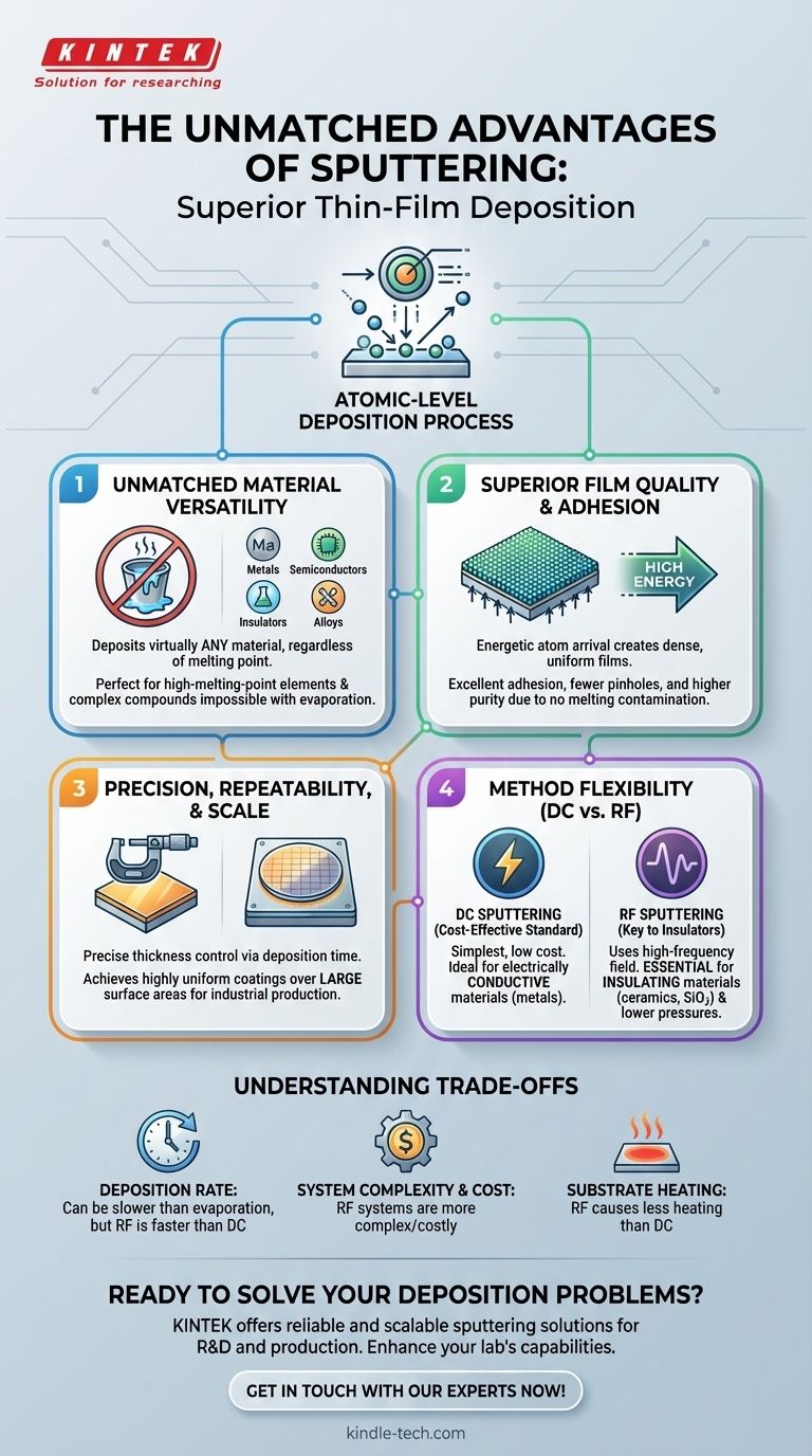
At its core, sputtering is a physical vapor deposition (PVD) method prized for its exceptional versatility and the superior quality of the films it produces. Its primary advantages lie in its ability to deposit a vast range of materials—including those difficult to evaporate—while achieving excellent adhesion, high purity, and precise, uniform thickness control over large areas.
Sputtering's fundamental advantage is its process of atomic-level deposition. By using energetic ion bombardment instead of heat, it produces dense, highly adherent, and pure thin films from virtually any target material, making it a reliable and scalable solution for advanced manufacturing and research.
Why Choose Sputtering? The Core Benefits
Sputtering stands apart from other deposition techniques, like thermal evaporation, due to the unique physics of its process. This translates into tangible benefits in material capability, film quality, and process control.
Unmatched Material Versatility
The most significant advantage of sputtering is its ability to deposit films from nearly any substance. Because it mechanically ejects atoms from a target rather than boiling them, material melting point is not a limiting factor.
This allows for the deposition of elements and compounds with extremely high melting points and low vapor pressures, which are impossible to handle with standard evaporation methods.
You can effectively sputter metals, semiconductors, insulators, and complex mixtures or alloys, using a solid target of any shape.
Superior Film Quality and Adhesion
Sputtered atoms arrive at the substrate with much higher kinetic energy than evaporated atoms. This energy has a profound impact on the quality of the resulting film.
The high energy promotes excellent adhesion between the film and the substrate, often creating a thin diffusion layer at the interface that locks the coating in place.
This process also results in dense, uniform films with fewer pinholes or defects. Since sputtering does not require melting a source material in a crucible, it avoids a common source of contamination, leading to higher film purity.
Precision, Repeatability, and Scale
Sputtering offers an exceptional degree of process control, making it ideal for applications that demand high precision and reproducibility.
Film thickness is directly proportional to the deposition time and the target current or power. This relationship allows for precise and repeatable control over the final thickness.
Furthermore, the process can be engineered to create highly uniform films over very large surface areas, a critical requirement for industrial-scale production in fields like semiconductors and architectural glass.
Understanding the Sputtering Methods: DC vs. RF
The general advantages of sputtering are enhanced or modified depending on the specific technique used. The most common distinction is between Direct Current (DC) and Radio Frequency (RF) sputtering.
DC Sputtering: The Cost-Effective Standard
DC sputtering is the simplest and most economical form of the technology. It uses a direct current power source to generate the plasma.
Its primary advantage is its low cost and ease of control, making it the go-to method for depositing electrically conductive materials, such as metals and transparent conductive oxides.
RF Sputtering: The Key to Insulators
RF sputtering uses a high-frequency alternating electric field. This innovation is crucial because it allows for the deposition of electrically insulating (dielectric) materials like ceramics, silica (SiO2), or alumina.
In RF sputtering, the alternating field prevents charge build-up on the insulating target, which would otherwise halt the DC process.
It also operates at much lower gas pressures (e.g., 1-15 mTorr) compared to DC. This reduces the chance of gas atoms becoming incorporated as impurities in the film and improves the "line of sight" for sputtered atoms, enhancing film quality.
Understanding the Trade-offs
While powerful, sputtering is not without its considerations. Understanding its limitations is key to making an informed decision.
Deposition Rate
Sputtering is a very controlled process, but this can sometimes mean it is slower than high-rate thermal evaporation techniques, especially for certain metals like aluminum. However, RF sputtering can offer deposition rates up to 10 times higher than DC sputtering at similar pressures.
System Complexity and Cost
Sputtering systems, particularly those using RF power supplies and sophisticated magnetic confinement, are generally more complex and carry a higher initial cost than simple thermal evaporators. DC systems remain a cost-effective exception for conductive films.
Substrate Heating
The bombardment of the substrate by energetic particles can cause significant heating. While this can improve film density, it may damage heat-sensitive substrates. RF sputtering tends to cause less substrate heating than DC methods.
Making the Right Choice for Your Goal
Your choice of sputtering technique should be driven by the material you need to deposit and your budget.
- If your primary focus is cost-effective metal coating: DC sputtering is the most direct and economical solution for conductive targets.
- If your primary focus is depositing insulating or dielectric materials: RF sputtering is the essential and superior choice, as DC sputtering will not work.
- If your primary focus is R&D or creating complex alloy films: An advanced technique like confocal sputtering allows for co-deposition from multiple targets to engineer novel materials.
Ultimately, sputtering empowers you to create high-quality, durable thin films from the widest possible range of materials, solving challenges that other methods cannot.
Summary Table:
| Key Advantage | Description |
|---|---|
| Material Versatility | Deposits virtually any material, including high-melting-point metals and insulators, unlike evaporation methods. |
| Superior Film Quality | Produces dense, uniform films with excellent adhesion and high purity due to atomic-level, energetic deposition. |
| Precision & Control | Enables precise, repeatable thickness control and uniform coatings over large areas for scalable production. |
| Method Flexibility | DC sputtering for cost-effective metal coatings; RF sputtering for essential deposition of insulating materials. |
Ready to solve your most challenging thin-film deposition problems?
Sputtering technology from KINTEK provides the material versatility and film quality your R&D or production process demands. Whether you need to deposit complex alloys, delicate insulators, or high-purity metals, our expertise in lab equipment ensures you get a reliable and scalable solution.
Contact KINTEK today to discuss how our sputtering systems can enhance your laboratory's capabilities and drive your innovations forward.
Get in touch with our experts now!
Visual Guide
Related Products
- Lab Sterile Slapping Type Homogenizer for Tissue Mashing and Dispersing
- Spark Plasma Sintering Furnace SPS Furnace
- Single Punch Manual Tablet Press Machine TDP Tablet Punching Machine
People Also Ask
- What role does an ultrasonic cleaner play in the pre-treatment of 4140 steel? Ensure Uniform Nitriding Activation
- What is the primary function of an ultrasonic cleaner in coating? Achieve Unmatched Substrate Purity for PVD Adhesion
- What role does a laboratory homogenizer play in radioactive cesium detection? Ensure Accuracy in Wildlife Sampling
- Why is it necessary to use an ultrasonic cell disruptor before yeast flow cytometry? Ensure Data Accuracy
- How does a laboratory automatic masticator or homogenizer facilitate the processing of biofilm samples? Optimize Accuracy


