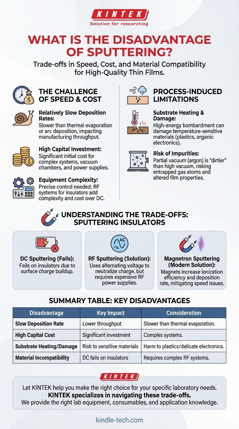
At its core, the primary disadvantages of sputtering are its relatively slow deposition rates, high initial equipment costs, and the potential for process-induced damage to sensitive materials. It is a more complex and expensive process compared to simpler methods like thermal evaporation, and its most basic form is incompatible with electrically insulating materials.
While sputtering is renowned for producing high-quality, dense thin films, it is not a universally optimal solution. Understanding its limitations in speed, cost, and material compatibility is critical to determining if it's the right choice for your specific application.
The Challenge of Speed and Cost
Sputtering often involves a trade-off where higher film quality is exchanged for lower throughput and higher operational complexity.
Relatively Slow Deposition Rates
Sputtering is generally a slower thin-film deposition method when compared directly to techniques like thermal evaporation or arc deposition.
The process of physically knocking atoms off a target with ions is inherently less rapid than boiling a material. For certain materials, like silicon dioxide (SiO2), the sputter rate can be particularly low, impacting manufacturing throughput.
High Capital Investment
Sputtering systems represent a significant capital expense. The need for a robust vacuum chamber, high-voltage power supplies, process gas control, and cooling systems drives up the initial cost.
This high barrier to entry makes sputtering less suitable for small-scale lab work or applications where cost is the primary driver.
Equipment Complexity
The process requires precise control over multiple variables, including gas pressure, power, and substrate temperature.
Furthermore, sputtering insulating materials requires specialized Radio Frequency (RF) power supplies and impedance-matching networks, adding another layer of complexity and cost compared to standard Direct Current (DC) systems.
Process-Induced Limitations
The high-energy nature of the sputtering process, while beneficial for film density and adhesion, can also introduce undesirable side effects.
Substrate Heating and Damage
The bombardment of the target by ions and the subsequent travel of high-energy atoms toward the substrate can cause significant substrate heating.
This can be detrimental when coating temperature-sensitive materials, such as plastics or organic electronics. The energetic ion bombardment can also physically damage delicate materials, degrading their properties.
Risk of Impurities
Sputtering operates in a partial vacuum, requiring a process gas like argon. This environment is "dirtier" than the high vacuum used in evaporation.
As a result, there is a greater risk of process gas atoms or other residual gases becoming entrapped in the growing film, which can alter its electrical or optical properties.
Understanding the Trade-offs: Sputtering Insulators
One of the most significant historical limitations of sputtering defines the different types of systems used today.
The Insulator Problem: Why DC Sputtering Fails
The most basic method, DC sputtering, works by applying a negative DC voltage to the target material. This attracts positive gas ions, which strike the target and eject atoms.
This only works for conductive targets. If the target is an electrical insulator (a dielectric), positive charge from the ions quickly accumulates on its surface. This "charge-up" effect repels incoming positive ions, effectively poisoning the target and stopping the process entirely.
The RF Solution and Its Drawbacks
To overcome this, RF sputtering was developed. It uses an alternating, high-frequency voltage. During one half of the cycle, the target is bombarded by ions; during the other half, it is bombarded by electrons, which neutralizes the positive charge buildup.
While effective, this solution requires the complex and expensive RF power supplies mentioned earlier, making it a significant trade-off between capability and cost.
The Rise of Magnetron Sputtering
Modern systems almost universally use magnetron sputtering. By adding powerful magnets behind the target, the plasma is confined near the target surface. This dramatically increases the ionization efficiency and, as a result, the deposition rate, mitigating one of the core weaknesses of basic sputtering.
Making the Right Choice for Your Application
Selecting a deposition method requires balancing your technical goals with practical constraints.
- If your primary focus is high throughput and low cost: Sputtering may not be ideal; consider thermal evaporation, especially for simple metals.
- If your primary focus is coating sensitive organic or plastic substrates: You must carefully control the sputtering process to mitigate substrate heating or consider a lower-energy deposition method.
- If your primary focus is coating insulating materials (ceramics, oxides): You must use an RF sputtering system, accepting the associated increase in cost and complexity over a DC system.
- If your primary focus is the highest possible film quality (density and adhesion): Sputtering is an excellent choice, but you must accept the trade-offs in speed and cost.
Ultimately, choosing sputtering is a deliberate decision to prioritize film quality and material versatility over speed and simplicity.
Summary Table:
| Disadvantage | Key Impact | Consideration |
|---|---|---|
| Slow Deposition Rate | Lower manufacturing throughput | Slower than thermal evaporation for some materials |
| High Capital Cost | Significant initial investment | Complex vacuum, power, and cooling systems |
| Substrate Heating/Damage | Risk to temperature-sensitive materials | Energetic process can harm plastics or delicate electronics |
| Material Incompatibility | DC sputtering fails on insulators | Requires complex RF systems for ceramics/oxides |
Choosing the right thin-film deposition method is critical to your project's success.
While sputtering has disadvantages, its ability to produce high-quality, dense films is unmatched for many applications. The experts at KINTEK specialize in helping laboratories and manufacturers navigate these trade-offs. We provide the right lab equipment and consumables, along with deep application knowledge, to ensure your process is optimized for quality, efficiency, and cost.
Let KINTEK help you make the right choice. Contact our experts today for a personalized consultation on your specific laboratory needs.
Visual Guide
Related Products
- Spark Plasma Sintering Furnace SPS Furnace
- Lab Sterile Slapping Type Homogenizer for Tissue Mashing and Dispersing
People Also Ask
- What is the theory of spark plasma sintering? A Guide to Rapid, Low-Temperature Densification
- What are the advantages of CAMI/SPS for W-Cu composite preparation? Reduce cycles from hours to seconds.
- What are the fundamentals of spark plasma sintering process? Unlock Rapid, High-Performance Material Consolidation
- What is the process fundamentals of spark plasma sintering? Achieve Rapid, High-Density Material Consolidation
- What is the difference between spark plasma sintering and flash sintering? A Guide to Advanced Sintering Methods

