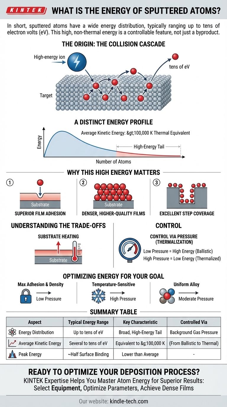
In short, sputtered atoms have a wide energy distribution, typically ranging up to tens of electron volts (eV). This kinetic energy is significantly higher than that of atoms in conventional thermal processes and is the primary reason sputtering produces dense, well-adhered thin films. A small fraction of these atoms can also be ionized, further influencing the deposition process.
The key takeaway is that the high, non-thermal energy of sputtered atoms is a controllable feature, not just a byproduct. By adjusting parameters like gas pressure, you can tune this energy to achieve specific film properties, from exceptional adhesion to minimized substrate heating.
The Origin of Sputtered Atom Energy
To understand the practical implications of sputtered atom energy, we must first understand its source. It is not a result of heat, but of direct momentum transfer.
The Collision Cascade
Sputtering begins when a high-energy ion, accelerated from a plasma, strikes a solid target material. This initial impact is far more energetic than a typical thermal interaction, often involving voltages of 3-5 kV in DC sputtering.
This impact sets off a chain reaction within the target, a "collision cascade," where atoms knock into their neighbors. This cascade of momentum transfer eventually reaches the surface, and if an atom at the surface receives enough energy to overcome the material's surface binding energy, it is ejected.
A Distinct Energy Profile
The resulting energy of these ejected, or "sputtered," atoms is not a single value but a broad distribution.
The distribution typically peaks at a relatively low energy—around half the surface binding energy of the target material. However, it features a long "high-energy tail," meaning a significant number of atoms are ejected with much higher energies.
This results in an average kinetic energy that is often an order of magnitude higher than the peak of the distribution, typically in the range of several to tens of eV. For perspective, this is equivalent to a thermal temperature of over 100,000 K.
Why This High Energy Matters
The unique energy profile of sputtered atoms directly translates into the desirable characteristics of sputtered thin films, distinguishing the process from lower-energy methods like thermal evaporation.
Superior Film Adhesion
When a high-energy sputtered atom strikes the substrate, it doesn't just gently land. Its kinetic energy allows it to physically implant into the very first atomic layers of the surface.
This creates a strong, intermixed interface layer, resulting in far superior film adhesion compared to evaporated atoms, which have only low thermal energy and form a more distinct boundary.
Denser, Higher-Quality Films
The impact energy also promotes surface mobility. An arriving atom has enough energy to move around on the substrate surface for a short time before settling into a stable position.
This allows atoms to find and fill microscopic voids, resulting in films that are significantly denser, less porous, and often have better optical and electrical properties.
Excellent Step Coverage
While sputtering is often considered a line-of-sight process, the energetic particles arrive at the substrate from a wider range of angles due to gas scattering. This, combined with the high surface mobility, allows sputtered films to conform better to complex surface topographies, providing better coverage over sharp steps and inside trenches.
Understanding the Trade-offs
The high energy of sputtered atoms is a powerful tool, but it also introduces challenges that must be managed for successful deposition.
Substrate Heating
The constant bombardment of energetic atoms is an efficient way to transfer energy to the substrate. This kinetic energy is converted to heat, raising the substrate temperature during deposition.
This can be a significant problem for temperature-sensitive materials, such as plastics or certain electronic components, requiring active cooling or process adjustments.
Controlling Atom Energy with Pressure
The most effective tool for managing sputtered atom energy is the background gas pressure.
At very low pressures, sputtered atoms travel unimpeded to the substrate, arriving with their maximum energy. As pressure increases, these atoms undergo more collisions with the background gas, losing energy in a process called thermalization. By tuning the pressure, one can control the entire energy range, from high-energy ballistic impact to low-energy thermal motion.
The Risk of Resputtering
A small percentage of sputtered atoms are ionized. These ions can be accelerated by electric fields within the vacuum chamber and strike the growing film with high energy.
If this energy is sufficient, they can knock off, or "resputter," atoms that have already been deposited. This can alter the film's composition and create defects if not properly controlled.
Optimizing Energy for Your Goal
Controlling the energy of sputtered atoms is central to process engineering. The ideal energy depends entirely on the desired outcome for your thin film.
- If your primary focus is maximum film adhesion and density: Operate at lower gas pressures. This ensures atoms arrive at the substrate with high kinetic energy, promoting implantation and surface mobility.
- If your primary focus is depositing on a temperature-sensitive substrate: Use higher gas pressures. This thermalizes the sputtered atoms, reducing their impact energy and minimizing heat transfer to your substrate.
- If your primary focus is achieving uniform alloy composition: Moderate pressure is often best. It helps to average out the slight differences in energy and angular distribution between different sputtered elements.
Ultimately, mastering sputter deposition is about understanding and controlling the energy of the sputtered atom to build the precise film structure you require.
Summary Table:
| Aspect | Typical Energy Range | Key Characteristic |
|---|---|---|
| Energy Distribution | Up to tens of eV | Broad distribution with a high-energy tail |
| Peak Energy | ~Half the surface binding energy | Lower than the average energy |
| Average Kinetic Energy | Several to tens of eV | Equivalent to >100,000 K thermal energy |
| Controlled Via | Background gas pressure | From high-energy ballistic to low-energy thermal |
Ready to Optimize Your Thin Film Deposition Process?
At KINTEK, we specialize in providing advanced lab equipment and consumables for precise sputtering applications. Whether you need to achieve maximum film adhesion on robust substrates or deposit on temperature-sensitive materials, our expertise can help you master the energy of sputtered atoms for superior results.
We help you:
- Select the right sputtering equipment for your specific material and substrate requirements
- Optimize process parameters like gas pressure to control atom energy and film properties
- Achieve dense, well-adhered thin films with excellent step coverage
Contact us today to discuss how we can enhance your laboratory's thin film capabilities. Get in touch with our experts for a personalized consultation!
Visual Guide
Related Products
- Chemical Vapor Deposition CVD Equipment System Chamber Slide PECVD Tube Furnace with Liquid Gasifier PECVD Machine
- HFCVD Machine System Equipment for Drawing Die Nano-Diamond Coating
- 915MHz MPCVD Diamond Machine Microwave Plasma Chemical Vapor Deposition System Reactor
- RF PECVD System Radio Frequency Plasma-Enhanced Chemical Vapor Deposition RF PECVD
- Customer Made Versatile CVD Tube Furnace Chemical Vapor Deposition Chamber System Equipment
People Also Ask
- How expensive is chemical vapor deposition? Understanding the True Cost of High-Performance Coating
- What types of substrates are used in CVD to facilitate graphene films? Optimize Graphene Growth with the Right Catalyst
- What are the core advantages of PE-CVD in OLED encapsulation? Protect Sensitive Layers with Low-Temp Film Deposition
- What are the advantages of chemical vapor deposition? Achieve Superior Thin Films for Your Lab
- Why is Chemical Vapor Deposition (CVD) equipment uniquely suited for constructing hierarchical superhydrophobic structures?


