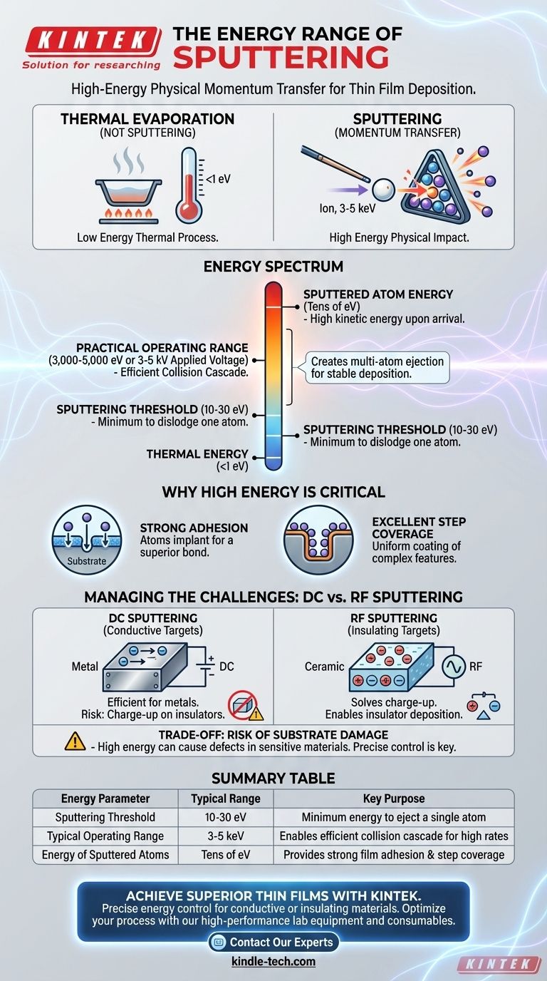
In practice, the kinetic energy of ions used in sputtering processes typically ranges from a few hundred to a few thousand electron volts (eV). For common DC sputtering systems, applied voltages of 3-5 kilovolts (kV) accelerate inert gas ions (like Argon) to energies of 3,000-5,000 eV. While the minimum energy required to dislodge a target atom is much lower, this higher energy range is used to ensure an efficient and stable deposition process.
Sputtering is not a thermal process like evaporation; it is a high-energy physical momentum transfer. Understanding this distinction is the key to grasping why it produces such durable, high-quality films and why different techniques like DC and RF sputtering exist.
The Physics of Sputtering: A Momentum Transfer Process
Sputtering works by bombarding a source material, known as the "target," with high-energy ions inside a vacuum chamber. These ions act like subatomic billiard balls, physically knocking atoms off the target surface. These ejected atoms then travel and deposit onto a "substrate," forming a thin film.
The Sputtering Threshold Energy
To eject an atom from a solid target, an incoming ion must have enough kinetic energy to overcome the target atom's surface binding energy. This minimum required energy is the sputtering threshold, which is typically in the range of 10 to 30 eV. This is significantly higher than the energies found in thermal processes (which are less than 1 eV).
The Typical Operating Range
While sputtering can occur at just a few tens of eV, practical systems operate at much higher energies to achieve a good deposition rate. Accelerating ions to 3,000-5,000 eV (3-5 keV) doesn't just knock out one atom; it initiates a collision cascade within the target material. This cascade ejects multiple target atoms for each incoming ion, dramatically increasing the efficiency of the process.
Why This High Energy is Critical
The high kinetic energy of the sputtered atoms as they travel to the substrate is responsible for the technique's key advantages.
- Strong Adhesion: Atoms arrive at the substrate with enough energy (tens of eV) to physically implant themselves into the surface layer, creating a much stronger bond than thermally evaporated films.
- Excellent Step Coverage: The collision cascade ejects target atoms in a wide range of directions, not just in a straight line. This allows the atoms to coat the sides of microscopic features on the substrate, leading to more uniform coverage.
Understanding the Trade-offs and Limitations
The high-energy nature of sputtering is a double-edged sword. It provides unique benefits but also introduces specific challenges that must be managed.
The Challenge with Insulating Materials
DC (Direct Current) sputtering works exceptionally well for conductive targets like metals. However, if you try to sputter an insulating material (like a ceramic or oxide), a problem arises. The positive ions from the plasma bombard the target, but the insulating material cannot dissipate this positive charge. This charge buildup, known as the "charge-up" effect, eventually repels subsequent positive ions, disrupting and stopping the sputtering process.
RF Sputtering: The Solution for Insulators
To overcome this, RF (Radio Frequency) sputtering is used. By applying a high-frequency AC voltage (commonly 13.56 MHz), the target's surface potential is rapidly alternated between negative and positive. During the brief positive cycle, it attracts electrons from the plasma, which neutralize the positive charge built up during the longer negative (sputtering) cycle. This allows for the continuous sputtering of non-conductive materials.
The Risk of Substrate Damage
The same energy that provides excellent adhesion can also cause damage. For very sensitive substrates or delicate film structures, the high-energy bombardment can introduce defects, stress, or unwanted mixing at interfaces. This requires careful control over process parameters like gas pressure and power to moderate the energy of the depositing species.
Making the Right Choice for Your Goal
Selecting the correct sputtering method depends entirely on the material you wish to deposit and your performance requirements.
- If your primary focus is depositing a metal or conductive film at a high rate: DC sputtering is the most direct and efficient method due to its simplicity and higher deposition rates.
- If your primary focus is depositing an insulating or dielectric material like an oxide or nitride: RF sputtering is the necessary choice to prevent the "charge-up" effect and maintain a stable process.
- If your primary focus is achieving the highest film quality and uniformity: You must precisely control process factors like gas pressure, power, and target-substrate distance, regardless of the sputtering type.
Ultimately, mastering sputtering requires recognizing that you are controlling a physical, energetic process to build films atom by atom.
Summary Table:
| Energy Parameter | Typical Range | Key Purpose |
|---|---|---|
| Sputtering Threshold | 10 - 30 eV | Minimum energy to eject a single atom |
| Typical Operating Range | 3,000 - 5,000 eV (3-5 keV) | Enables efficient collision cascade for high deposition rates |
| Energy of Sputtered Atoms | Tens of eV | Provides strong film adhesion and excellent step coverage |
Achieve Superior Thin Films with KINTEK
Whether you are depositing conductive metals with DC sputtering or delicate insulators with RF sputtering, precise energy control is paramount for film quality, adhesion, and uniformity. KINTEK specializes in high-performance lab equipment and consumables, providing the reliable sputtering solutions your laboratory needs to push the boundaries of materials science.
Let us help you optimize your process. Contact our experts today to discuss how our sputtering systems can bring durability and precision to your thin film applications.
Visual Guide