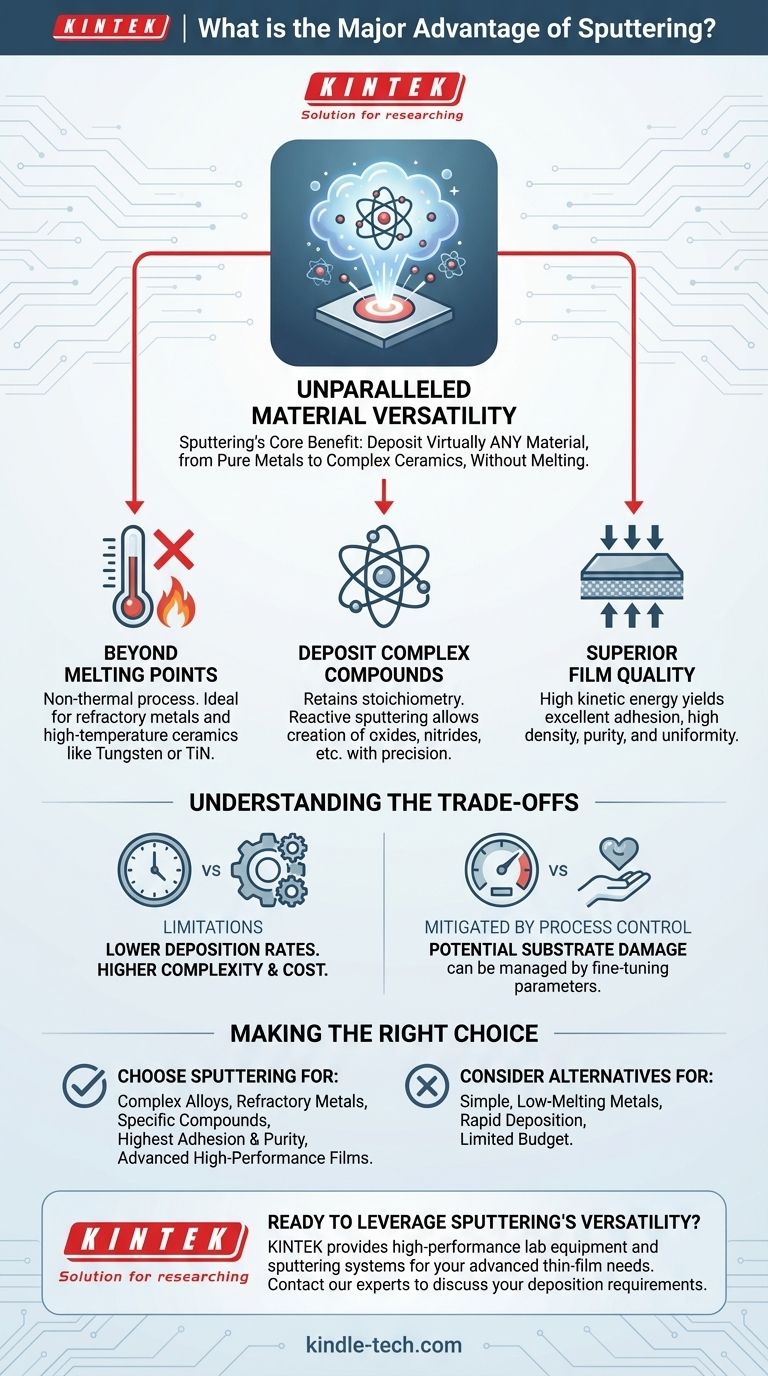
At its core, the single greatest advantage of sputtering is its unparalleled material versatility. Unlike methods that rely on melting, sputtering can deposit virtually any material—from pure metals and complex alloys to insulators and high-temperature ceramics—onto a substrate. This capability makes it the definitive choice for creating advanced, high-performance thin films.
Sputtering's primary advantage isn't just one feature, but how its core mechanism unlocks a combination of benefits. By physically ejecting atoms from a target, it sidesteps the chemical and thermal limitations of other methods, enabling the deposition of nearly any material with superior adhesion, density, and control.
Why Material Versatility is the Defining Advantage
Many thin-film deposition techniques, like thermal evaporation, are limited by the source material's properties. Sputtering’s physical nature fundamentally breaks through these barriers.
Sputtering Beyond Melting Points
Thermal evaporation works by heating a material until it vaporizes. This is inefficient or impossible for refractory metals and ceramics with extremely high melting points, such as tungsten or titanium nitride.
Sputtering is a non-thermal process. It uses high-energy ion bombardment to physically "knock" atoms loose from a target material. Because it doesn't rely on melting, a material's melting point becomes largely irrelevant.
Depositing Complex Compounds and Alloys
Sputtering excels at maintaining the original composition of a source material. When sputtering an alloy, the resulting film retains the same stoichiometry as the target, which is critical for applications requiring specific material properties.
Furthermore, reactive sputtering allows for the creation of new compound films on the fly. By introducing a reactive gas like nitrogen or oxygen into the vacuum chamber, one can deposit films like titanium nitride (TiN) or aluminum oxide (Al2O3) with precise control, starting from a pure metal target.
The Foundation for High-Quality Films
The high-energy plasma environment that enables this versatility is also directly responsible for the superior quality of sputtered films. This isn't a coincidence; the two advantages are directly linked by the physics of the process.
The Key Process Outcomes of Sputtering
Sputtering's unique mechanism produces films with a combination of desirable characteristics that are difficult to achieve simultaneously with other methods.
Superior Adhesion and Density
Sputtered atoms arrive at the substrate with significantly higher kinetic energy than evaporated atoms. This energy helps them form a stronger, more durable bond with the substrate surface, resulting in excellent adhesion.
This high energy also promotes the growth of a denser film structure with fewer voids or pinholes. This is critical for protective coatings, optical films, and electronic components where film integrity is paramount.
Exceptional Purity and Uniformity
Sputtering is performed in a high-vacuum environment, minimizing the risk of contamination from residual gases and resulting in high-purity films.
The process also offers exceptional control over film thickness. By precisely managing parameters like deposition time and target current, sputtering can produce films with excellent uniformity over very large areas, making it ideal for mass production of wafers and other large substrates.
Understanding the Trade-offs
No process is perfect. To make an informed decision, you must understand sputtering's limitations.
Lower Deposition Rates
In some cases, sputtering can have a slower deposition rate compared to high-rate thermal evaporation processes. For simple applications where speed is the only priority, other methods might be more efficient.
Process Complexity and Cost
Sputtering systems are mechanically complex. They require high-vacuum chambers, specialized power supplies, gas handling systems, and often, powerful magnets (magnetron sputtering). This results in higher initial equipment cost and maintenance complexity compared to simpler deposition setups.
Potential for Substrate Damage
The high-energy ion bombardment that provides so many benefits can also be a drawback. For extremely delicate substrates, this energy can sometimes induce stress or damage. However, this can often be mitigated by fine-tuning process parameters.
Making the Right Choice for Your Goal
Selecting a deposition method depends entirely on your technical requirements and project constraints.
- If your primary focus is depositing complex alloys, refractory metals, or specific compounds (like oxides or nitrides): Sputtering is almost certainly the superior choice due to its unmatched material versatility.
- If your primary focus is achieving the highest film adhesion, density, and purity for a high-performance application: Sputtering's high-energy process provides a distinct and measurable advantage over low-energy evaporation.
- If your primary focus is rapid deposition of a simple, low-melting-point metal on a limited budget: A simpler technique like thermal evaporation might be a more practical and cost-effective solution.
Ultimately, sputtering's power lies in its ability to transform nearly any material into a high-performance, precisely controlled thin film.
Summary Table:
| Feature | Sputtering Advantage |
|---|---|
| Material Versatility | Deposits pure metals, alloys, ceramics, and insulators. |
| Process Type | Non-thermal, physical vapor deposition (PVD). |
| Film Quality | Superior adhesion, high density, and excellent purity. |
| Composition Control | Maintains target stoichiometry for alloys and compounds. |
| Key Limitation | Lower deposition rates and higher system complexity vs. some methods. |
Ready to leverage sputtering's material versatility for your lab's thin-film applications?
KINTEK specializes in high-performance lab equipment, including sputtering systems, to help you deposit complex alloys, refractory metals, and precise compounds with superior film quality. Our expertise ensures you get the right solution for creating advanced, high-performance thin films.
Contact our experts today to discuss your specific deposition needs and discover how KINTEK can enhance your laboratory's capabilities.
Visual Guide
Related Products
- Lab Sterile Slapping Type Homogenizer for Tissue Mashing and Dispersing
- Spark Plasma Sintering Furnace SPS Furnace
- Single Punch Manual Tablet Press Machine TDP Tablet Punching Machine
People Also Ask
- How does a homogenizer affect the quality of electrode slurry? Master Battery Consistency with High-Shear Mixing
- What role does an ultrasonic cleaner play in the pre-treatment of 4140 steel? Ensure Uniform Nitriding Activation
- What role does a laboratory homogenizer play in radioactive cesium detection? Ensure Accuracy in Wildlife Sampling
- How does a laboratory automatic masticator or homogenizer facilitate the processing of biofilm samples? Optimize Accuracy
- Why is maintaining nanoparticle dispersion critical for photocatalytic reactors? Maximize Your Reaction Efficiency


