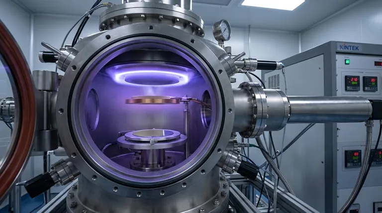
In essence, sputtering is a physical vapor deposition (PVD) process where atoms are ejected from a solid target material by bombarding it with high-energy ions inside a vacuum. These ejected atoms then travel and deposit onto a substrate, forming an extremely thin, uniform film. The entire process functions like a highly controlled, atomic-scale sandblasting operation.
Sputtering is fundamentally a momentum transfer process. It uses an energized inert gas, like Argon, to create ions that physically knock atoms off a source material (the target), which then re-condense as a high-quality coating on another surface (the substrate).
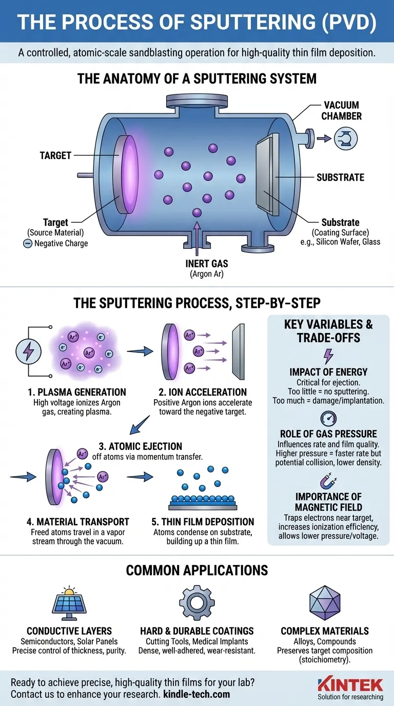
The Anatomy of a Sputtering System
To understand the process, you must first understand the key components at play within the system. Each element has a distinct and critical role.
The Vacuum Chamber
The entire process takes place inside a sealed chamber. The first step is to create a vacuum, pumping out air and other residual gases to remove moisture and impurities that could contaminate the final film.
The Target
This is the source material you wish to deposit as a film. The target is given a strong negative electrical charge.
The Substrate
This is the object or material that will be coated. Common substrates include silicon wafers, glass, or plastics, which are positioned to face the target.
The Inert Gas
An inert gas, most commonly Argon (Ar), is introduced into the vacuum chamber after the initial pump-down. This gas acts as the "ammunition" for the process, as it will be ionized to bombard the target.
The Sputtering Process, Step-by-Step
Once the components are in place, the process unfolds in a precise sequence of events driven by physics.
Step 1: Plasma Generation
A high voltage is applied within the chamber. This powerful electric field energizes the Argon gas, stripping electrons from the Argon atoms and creating a plasma—a glowing, ionized gas composed of positively charged Argon ions (Ar+) and free electrons.
Step 2: Ion Acceleration
The negatively charged target material strongly attracts the newly formed, positively charged Argon ions. These ions accelerate across the chamber and slam into the target surface at high velocity.
Step 3: Atomic Ejection
The impact of an Argon ion on the target is a pure momentum transfer event. If the ion strikes with enough kinetic energy to overcome the binding energy holding the target's atoms together, it causes a "collision cascade," knocking atoms or molecules loose from the target material.
Step 4: Material Transport
These newly freed atoms from the target travel in a vapor stream through the low-pressure environment of the chamber.
Step 5: Thin Film Deposition
The ejected target atoms eventually reach the substrate, where they land and condense. Over time, these atoms build up, layer by layer, to form a thin, solid, and highly uniform film with specific, desirable properties.
Understanding the Key Variables and Trade-offs
The quality and characteristics of the sputtered film are not accidental. They are the direct result of carefully managing the process parameters. Simply running the process is not enough; controlling it is what yields results.
The Impact of Energy
The energy of the bombarding ions is critical. Too little energy, and no atoms will be ejected from the target. Too much energy can cause damage or implant the ions into the target instead of sputtering it effectively.
The Role of Gas Pressure
The pressure of the Argon gas inside the chamber influences the process significantly. Higher pressure can increase the sputtering rate but may also cause sputtered atoms to collide with gas atoms on their way to the substrate, reducing the film's density and quality.
The Importance of a Magnetic Field
Many modern systems use magnets behind the target (a technique called magnetron sputtering). This magnetic field traps electrons near the target surface, dramatically increasing the efficiency of Argon ionization and allowing the process to run at lower pressures and voltages.
How to Apply This to Your Goal
Sputtering is chosen for its precision and versatility. The right application depends entirely on the desired outcome for the final film.
- If your primary focus is producing reflective or electrically conductive layers (like in semiconductors or solar panels): Sputtering provides exceptional control over film thickness, purity, and electrical resistivity.
- If your primary focus is creating hard, durable, or biocompatible coatings (for cutting tools, medical implants, or optics): The momentum-driven deposition creates dense, well-adhered films that are highly resistant to wear.
- If your primary focus is depositing complex materials like alloys or compounds: Sputtering is excellent at preserving the original composition (stoichiometry) of the target material in the deposited film.
Ultimately, sputtering empowers engineers and scientists to construct materials one atomic layer at a time, building high-performance surfaces from the ground up.
Summary Table:
| Key Component | Role in the Process |
|---|---|
| Vacuum Chamber | Sealed environment free of contaminants |
| Target | Source material to be deposited (negatively charged) |
| Substrate | Surface to be coated (e.g., silicon, glass) |
| Inert Gas (Argon) | Ionized to bombard the target |
| Process Step | Description |
| Plasma Generation | Electric field ionizes Argon gas |
| Ion Acceleration | Positively charged ions accelerate toward target |
| Atomic Ejection | Ions knock atoms from target via momentum transfer |
| Material Transport | Freed atoms travel through vacuum |
| Film Deposition | Atoms condense on substrate, forming a thin layer |
Ready to achieve precise, high-quality thin films for your lab?
Sputtering is a cornerstone technique for creating uniform conductive, durable, or complex material coatings essential in semiconductor, optical, and medical applications. At KINTEK, we specialize in providing advanced lab equipment and consumables tailored to your specific deposition needs. Our expertise ensures you get the right sputtering solutions for superior film adhesion, purity, and performance.
Contact us today to discuss how our sputtering systems can enhance your research and production outcomes!
Visual Guide
Related Products
- Spark Plasma Sintering Furnace SPS Furnace
- Vacuum Induction Melting Spinning System Arc Melting Furnace
- Chemical Vapor Deposition CVD Equipment System Chamber Slide PECVD Tube Furnace with Liquid Gasifier PECVD Machine
- Customer Made Versatile CVD Tube Furnace Chemical Vapor Deposition Chamber System Equipment
People Also Ask
- What is the pressure for spark plasma sintering? A Guide to Optimizing SPS Parameters
- What is the mechanism of SPS process? A Deep Dive into Rapid, Low-Temperature Sintering
- What is the theory of spark plasma sintering? A Guide to Rapid, Low-Temperature Densification
- What technical advantages does a Spark Plasma Sintering (SPS) furnace offer for LZP ceramics? Enhance Ionic Conductivity
- What is the difference between spark plasma sintering and flash sintering? A Guide to Advanced Sintering Methods


