Application of Precious Metal Targets
Role in Semiconductor Manufacturing
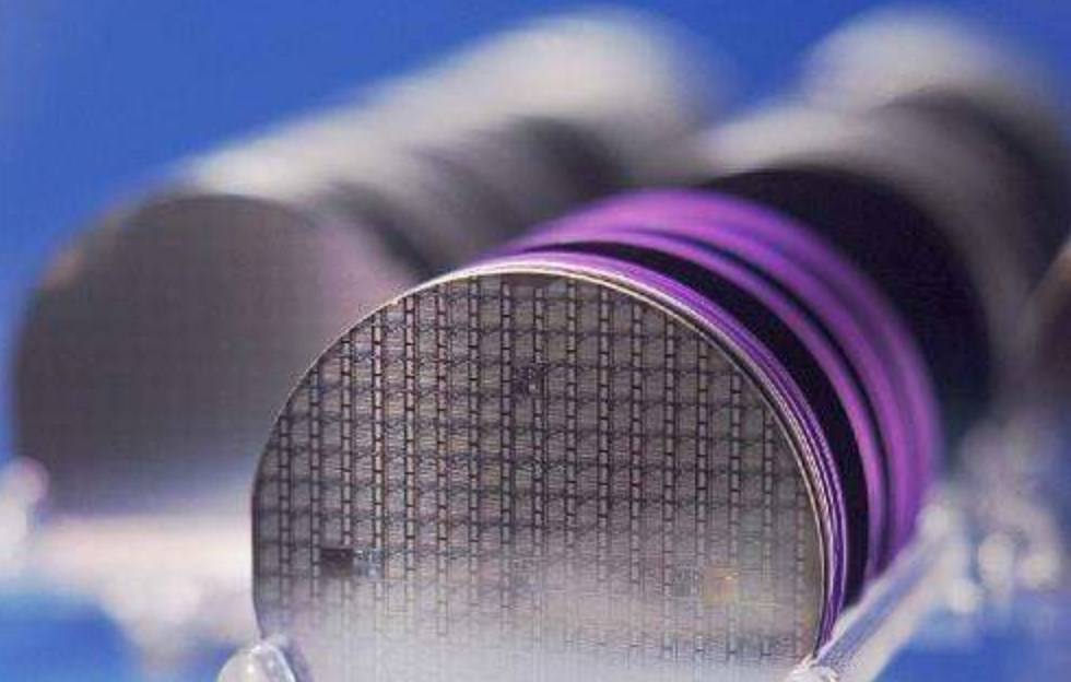
Precious metal targets, such as gold, silver, platinum, and ruthenium, play a pivotal role in the intricate processes of semiconductor manufacturing. These metals, along with their alloys, are integral components in the creation of ultra-large-scale integrated circuits (ULSIs) and advanced chip packaging technologies. Their applications extend to serving as interconnecting materials and backside coatings, which are essential for the functionality and reliability of semiconductor devices.
The use of precious metal targets has surged in recent years, driven by the relentless advancements in semiconductor technology. These materials are particularly valued for their superior electrical conductivity, thermal stability, and corrosion resistance, which are critical attributes in the high-precision environments of semiconductor fabrication. For instance, gold and silver are extensively used in wire bonding and as conductive layers, while platinum and ruthenium find applications in diffusion barriers and as seed layers for electroplating.
The evolution of chip packaging technologies has further amplified the demand for these precious metals. Advanced packaging techniques, such as 3D stacking and wafer-level packaging, require materials that can withstand the complex thermal and mechanical stresses involved. Precious metal targets meet these stringent requirements, ensuring the integrity and performance of the final semiconductor products.
In summary, the role of precious metal targets in semiconductor manufacturing is multifaceted and indispensable. Their unique properties and adaptability make them essential components in the development of cutting-edge semiconductor technologies, driving the industry forward with each innovation.
Specific Applications
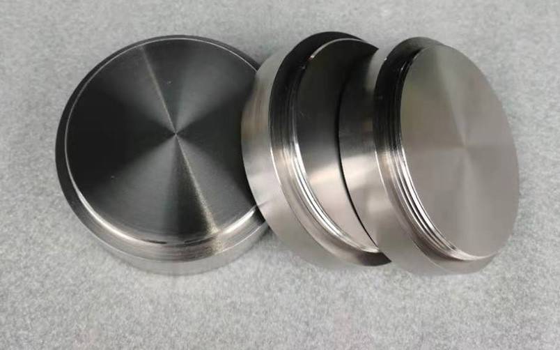
Precious metal sputtering targets play a pivotal role in the semiconductor manufacturing process, serving a variety of critical functions that enhance the performance and reliability of electronic devices. These targets, which include gold, silver, platinum, ruthenium, and their alloys, are meticulously detailed in Table 9-26, illustrating their diverse applications within the industry.
In the realm of ultra-large-scale integrated circuits (ULSI), precious metal targets are employed as interconnecting materials, ensuring efficient electrical conductivity between different components. This application is particularly crucial in advanced chip packaging technologies, where the integrity of these connections directly impacts the overall functionality and speed of the semiconductor devices.
Moreover, these targets are utilized for backside coatings, providing robust protection against environmental factors and mechanical stress. This dual role of interconnecting and protecting underscores the indispensable nature of precious metal targets in modern semiconductor manufacturing.
Table 9-26 provides a comprehensive overview of the specific uses of these targets, highlighting their versatility and the intricate processes they facilitate. From enhancing the conductivity of microelectronic components to fortifying the structural integrity of semiconductor devices, the applications of precious metal sputtering targets are as varied as they are essential.
Preparation of Precious Metal Targets
Methods for Low Melting Point Metals
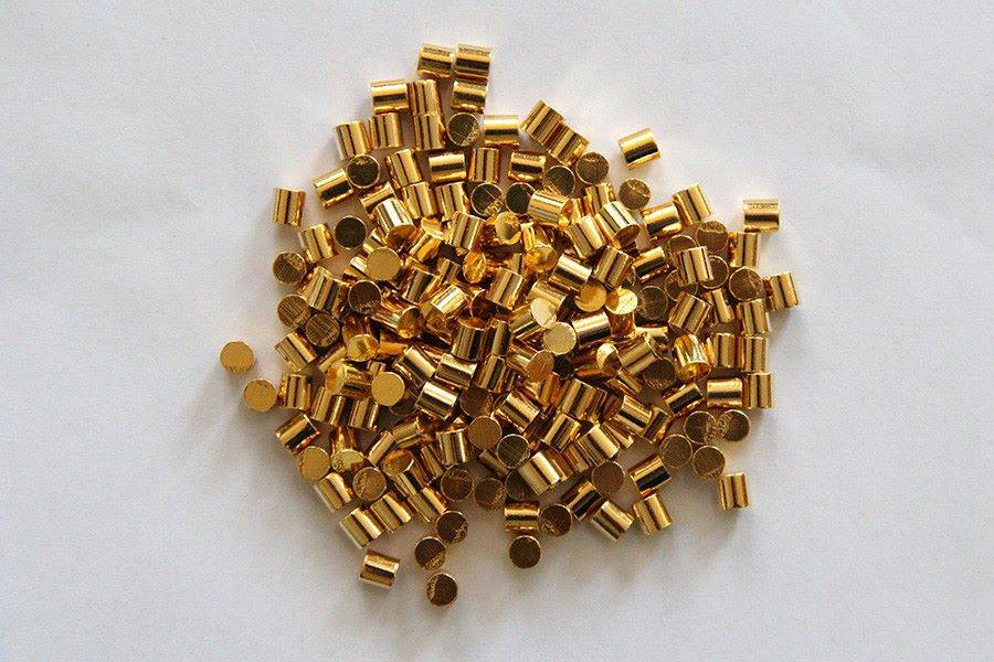
For metals such as gold, silver, and platinum, the preparation process begins with vacuum melting and casting. This initial step ensures the purity and homogeneity of the metal, which is crucial for their application in semiconductor manufacturing. Following the casting, the metals undergo rolling and pressure processing. These techniques are essential for shaping the metals into the precise dimensions and microstructures required for target materials.
Rolling is particularly effective in refining the grain size and orientation of the metals, which significantly impacts their performance in sputtering processes. Pressure processing, on the other hand, further enhances the mechanical properties and density of the target materials, ensuring they meet the stringent specifications needed in semiconductor production.
These methods not only facilitate the formation of target materials but also contribute to their overall quality and reliability. The combination of vacuum melting, casting, rolling, and pressure processing ensures that the final products are of the highest purity and consistency, making them ideal for use in advanced semiconductor technologies.
Methods for Refractory Metals
Refractory metals, such as ruthenium, molybdenum, tungsten, and tantalum, are distinguished by their exceptionally high melting points and resistance to wear, corrosion, and deformation. These properties make them indispensable in various high-temperature and high-stress applications, particularly in semiconductor manufacturing. The preparation of these metals often involves advanced techniques from the field of powder metallurgy.
One of the primary methods for preparing refractory metals is through vacuum hot pressure sintering or hot isostatic pressure sintering. These processes allow for the creation of dense, homogeneous materials with controlled microstructures, which are crucial for their performance in demanding applications. For instance, molybdenum, a commonly used refractory metal in vacuum furnaces, undergoes a significant increase in resistivity when heated, necessitating adjustments in the electrical control system to maintain optimal performance.
In contrast, tungsten, another refractory metal, can withstand even higher operating temperatures but is more costly. Despite its higher price, tungsten's superior thermal stability makes it a preferred choice in certain high-temperature environments. Additionally, graphite, while less costly than metallic elements, exhibits a decrease in electrical resistance when heated, offering an alternative for applications where cost and thermal properties are critical considerations.
| Metal | Common Use in Vacuum Furnaces | Resistivity Change with Heating |
|---|---|---|
| Molybdenum | Widely used | 5x increase |
| Tungsten | High-temperature use | Less significant increase |
| Graphite | Cost-effective alternative | 20% decrease |
The choice of material and preparation method depends on the specific requirements of the application, balancing factors such as cost, thermal stability, and electrical properties.
Microstructure Control
Microstructure control is a critical aspect in the preparation of precious metal targets, particularly in semiconductor manufacturing. For low melting point metals such as gold, silver, and platinum, the grain size and orientation are meticulously controlled through a combination of pressure processing and heat treatment. This dual approach ensures that the target materials exhibit the desired mechanical properties and uniformity, which are essential for their performance in semiconductor applications.
In contrast, refractory metals like ruthenium and its alloys require a different strategy due to their higher melting points and unique metallurgical properties. These metals are typically prepared using powder metallurgy techniques, where the size and distribution of powder particles play a pivotal role. The sintering process, whether through vacuum hot pressure sintering or hot isostatic pressure sintering, is optimized to achieve the necessary grain structure and density. This method ensures that the final target material is both durable and suitable for high-precision sputtering applications in semiconductor manufacturing.
The control of microstructure in both low melting point and refractory metals is not just about achieving a specific grain size or orientation; it is about tailoring the material to meet the stringent demands of semiconductor technology. Each step in the preparation process—from initial melting and casting to final sintering—is carefully calibrated to ensure that the target material meets the high standards required for reliable and efficient semiconductor production.
Recycling of Precious Metal Targets
Importance of Recycling
In semiconductor manufacturing, the efficient utilization of precious metal targets remains a significant challenge. Despite their critical role in the production of advanced integrated circuits, over 70% of these materials are left unutilized. This inefficiency results in substantial quantities of residual targets, trimmings, and scrap that must be managed effectively.
Recycling these materials is not just an environmental imperative but also a strategic economic decision. The process of recycling ensures that valuable resources are not wasted, thereby reducing the overall cost of production and minimizing the environmental impact associated with the extraction and processing of new materials.
Moreover, the recycling of precious metal targets in semiconductor manufacturing is essential for maintaining a sustainable supply chain. As the demand for semiconductors continues to grow, the ability to recover and reuse these materials becomes increasingly important. This practice not only conserves finite natural resources but also contributes to the long-term viability of the semiconductor industry.
In summary, the recycling of precious metal targets in semiconductor manufacturing is crucial for optimizing resource use, reducing costs, and ensuring the sustainability of the industry.
Physical Recycling Methods
Physical recycling methods play a crucial role in the recovery and reuse of precious metal targets in semiconductor manufacturing. These methods are designed to efficiently remove impurities and restore the targets to a usable condition.
One of the primary techniques involves mechanical processing, which includes crushing and sieving the residual targets. This step is essential for breaking down the targets into smaller, manageable pieces, making it easier to remove impurities. For instance, ruthenium targets are typically crushed into fine particles, which are then subjected to further purification processes.
Following mechanical processing, acid washing is employed to dissolve and remove any remaining impurities. This step ensures that the target material is thoroughly cleaned, enhancing its purity and reusability. Acid washing is particularly effective for refractory metals like ruthenium, which require stringent purification to maintain their structural integrity and performance in semiconductor applications.
In addition to acid washing, deoxidation and magnetic treatment are critical steps in the physical recycling process. Deoxidation helps to remove any residual oxygen, which can otherwise compromise the quality of the recycled material. Magnetic treatment, on the other hand, is used to separate any magnetic impurities that may be present, ensuring that the final product is free from contaminants.
These physical recycling methods are not only effective in restoring the targets for reuse but also contribute to the overall sustainability of semiconductor manufacturing. By maximizing the utilization of precious metal targets, these processes help to reduce waste and minimize the environmental impact associated with the production and disposal of these materials.
Chemical Recycling Methods
Chemical recycling methods play a crucial role in the recovery of precious metals from residual targets and scrap generated during semiconductor manufacturing. This process begins with the dissolution of these materials into a solution, which is a critical step to facilitate subsequent chemical treatments.
Once dissolved, the solution undergoes a series of intricate processes including chemical deposition, extraction, and adsorption. These steps are designed to selectively separate and concentrate the precious metals from other impurities present in the solution. Chemical deposition involves the formation of a solid phase from the dissolved metals, while extraction and adsorption techniques use specific reagents or materials to capture the target metals.
Following these initial stages, the concentrated precious metal solution is subjected to distillation, a process that further purifies the metals by removing volatile components and residual impurities. The final step in the chemical recycling process involves the decomposition or reduction of the purified metals. This is typically achieved through the use of hydrogen, which reduces the metal compounds back to their elemental form, yielding high-purity precious metals.
These high-purity metals are then ready for reuse in the semiconductor manufacturing process, thereby closing the loop on material utilization and significantly reducing waste.
Related Products
Related Articles
- Understanding Electrodes and Electrochemical Cells
- Pseudo-Reference Electrodes When and How to Use Them
- Design and Application of Reference Electrodes in Lithium Batteries
- Unlocking Purity: The Ultimate Guide to Handheld Precious Metal Analyzers
- Comprehensive Guide to Handheld Precious Metal Analyzers: Features, Applications, and Benefits