Yes, carbon can be sputtered, and it is a widely used industrial and research technique for depositing high-performance carbon thin films. This process, which typically uses a graphite target, is one of the primary methods for producing coatings known as amorphous carbon (a-C) and, more specifically, diamond-like carbon (DLC).
Sputtering carbon is not only possible, it is a foundational process in modern materials science. The core challenge is not if it can be done, but how to precisely control the sputtering energy and environment to engineer the carbon film's final properties, from soft and conductive to extremely hard and slick.

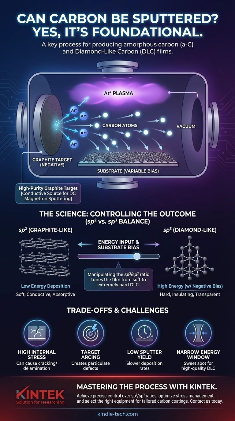
How Carbon Sputtering Works
Sputtering is a Physical Vapor Deposition (PVD) technique. Think of it as an atomic-scale sandblasting process where atoms, rather than grains of sand, are used to chip away at a target material.
The Graphite Target
The source material for sputtered carbon is almost always a high-purity graphite target. Graphite is chosen because it is a stable, solid form of carbon that is electrically conductive.
This conductivity is a major advantage, as it allows the use of DC magnetron sputtering, a fast, efficient, and highly common deposition method.
The Sputtering Mechanism
Inside a vacuum chamber, a gas—typically an inert one like Argon (Ar)—is introduced. A strong electric field ionizes this gas, creating a plasma.
These positively charged argon ions are accelerated with high energy toward the negatively charged graphite target. Upon impact, they knock carbon atoms loose from the target's surface. These ejected carbon atoms then travel through the vacuum and deposit onto a substrate, gradually building up a thin film.
The Resulting Film: Amorphous Carbon
The sputtered carbon atoms do not arrange themselves into a perfect crystal lattice like diamond or graphite. Instead, they form an amorphous carbon (a-C) film.
This film is a disordered network of carbon atoms connected by two different types of atomic bonds: sp² (graphite-like) and sp³ (diamond-like). The ratio of these two bond types dictates the film's final properties.
The sp² vs. sp³ Balance: Controlling the Outcome
The true power of sputtering carbon lies in the ability to manipulate the ratio of sp² to sp³ bonds, effectively tuning the film from "graphite-like" to "diamond-like."
Understanding sp² and sp³ Bonds
Think of sp² bonds as flat sheets of paper stacked on top of each other, like in graphite. They are strong within the sheet but slide easily against each other, making the material soft and electrically conductive.
sp³ bonds form a rigid, three-dimensional network, like a jungle gym. This structure, found in diamond, is what makes the material extremely hard, electrically insulating, and transparent.
Achieving Graphite-Like Films
When carbon atoms arrive at the substrate with low energy, they tend to arrange into the most stable configuration, which is the sp²-bonded, graphite-like structure. This results in a softer, more absorptive, and more conductive film.
Creating Diamond-Like Carbon (DLC)
To create a hard, diamond-like carbon (DLC) film, you must increase the energy of the carbon atoms as they deposit. This is most often done by applying a negative voltage (bias) to the substrate itself.
This bias attracts positive ions from the plasma to bombard the growing film. This bombardment provides the extra energy needed to force the carbon atoms into the less stable but much harder sp³-bonded configuration.
Understanding the Trade-offs and Challenges
While powerful, sputtering carbon is a delicate process with critical challenges that must be managed to achieve high-quality films.
High Internal Stress
The single biggest challenge with hard, high-sp³ DLC films is high internal compressive stress. The disordered, tightly packed sp³ structure pushes against itself, and if the stress becomes too high, the film can crack or peel off the substrate entirely. Managing this stress is crucial for adhesion and device reliability.
The Narrow Energy Window
There is a narrow "sweet spot" for the ion energy needed to form high-quality DLC.
- Too little energy results in a soft, sp²-rich, graphite-like film.
- Too much energy causes damage, breaking the desired sp³ bonds and converting them back into sp² bonds in a process called graphitization.
Finding and maintaining this optimal energy window is key to a repeatable process.
Low Sputter Yield
Carbon has a lower sputter yield than many metals. This means that for a given power and time, you will deposit a thinner film of carbon compared to a material like copper or titanium. Deposition rates can be a limiting factor in high-volume production.
Target Arcing
Graphite targets can be susceptible to arcing, where a sudden, localized discharge occurs on the target surface. Arcs can blast small particulates (macros) onto your substrate, creating defects that compromise the film's quality and performance.
Making the Right Choice for Your Goal
Your sputtering strategy should be directly aligned with the properties you need in your final carbon film.
- If your primary focus is a simple, electrically conductive coating: Use standard DC magnetron sputtering of a graphite target with low power and zero substrate bias.
- If your primary focus is maximum hardness and low friction: Use DC or HiPIMS sputtering with a carefully optimized negative substrate bias to promote sp³ bond formation while managing stress.
- If your primary focus is tuning optical or mechanical properties: Consider reactive sputtering by adding hydrogen (to create a-C:H) or nitrogen (for CNx) to the chamber to further modify the film's structure.
By mastering the energy and composition of your deposition, you can precisely engineer carbon films for a vast range of demanding applications.
Summary Table:
| Goal | Recommended Sputtering Method | Key Film Properties |
|---|---|---|
| Electrically Conductive Coating | Standard DC Magnetron (Low Power, No Bias) | Soft, Graphite-like (High sp²) |
| Maximum Hardness & Low Friction | DC/HiPIMS with Optimized Substrate Bias | Hard, DLC (High sp³) |
| Tuned Optical/Mechanical Properties | Reactive Sputtering (with H₂ or N₂) | Custom a-C:H or CNx films |
Ready to Engineer Your Next-Generation Carbon Coating?
At KINTEK, we specialize in advanced sputtering solutions for laboratory and research applications. Whether you need to deposit hard, wear-resistant DLC films or precisely tune conductive amorphous carbon coatings, our expertise and high-purity graphite targets ensure exceptional results.
We help you:
- Achieve precise control over sp²/sp³ bond ratios for tailored film properties.
- Optimize your process to manage internal stress and maximize adhesion.
- Select the right equipment and consumables for your specific application, from simple conductive layers to complex functional coatings.
Contact us today to discuss how our lab equipment and consumables can advance your materials research.
Visual Guide
Related Products
- Chemical Vapor Deposition CVD Equipment System Chamber Slide PECVD Tube Furnace with Liquid Gasifier PECVD Machine
- Customer Made Versatile CVD Tube Furnace Chemical Vapor Deposition Chamber System Equipment
- Graphite Vacuum Furnace Bottom Discharge Graphitization Furnace for Carbon Materials
- RF PECVD System Radio Frequency Plasma-Enhanced Chemical Vapor Deposition RF PECVD
- Spark Plasma Sintering Furnace SPS Furnace
People Also Ask
- How expensive is chemical vapor deposition? Understanding the True Cost of High-Performance Coating
- What are the advantages of chemical vapor deposition? Achieve Superior Thin Films for Your Lab
- What are the processes of vapor phase deposition? Understand CVD vs. PVD for Superior Thin Films
- What is plasma enhanced chemical vapor deposition PECVD equipment? A Guide to Low-Temperature Thin Film Deposition
- How are carbon nanotubes grown? Master Scalable Production with Chemical Vapor Deposition


