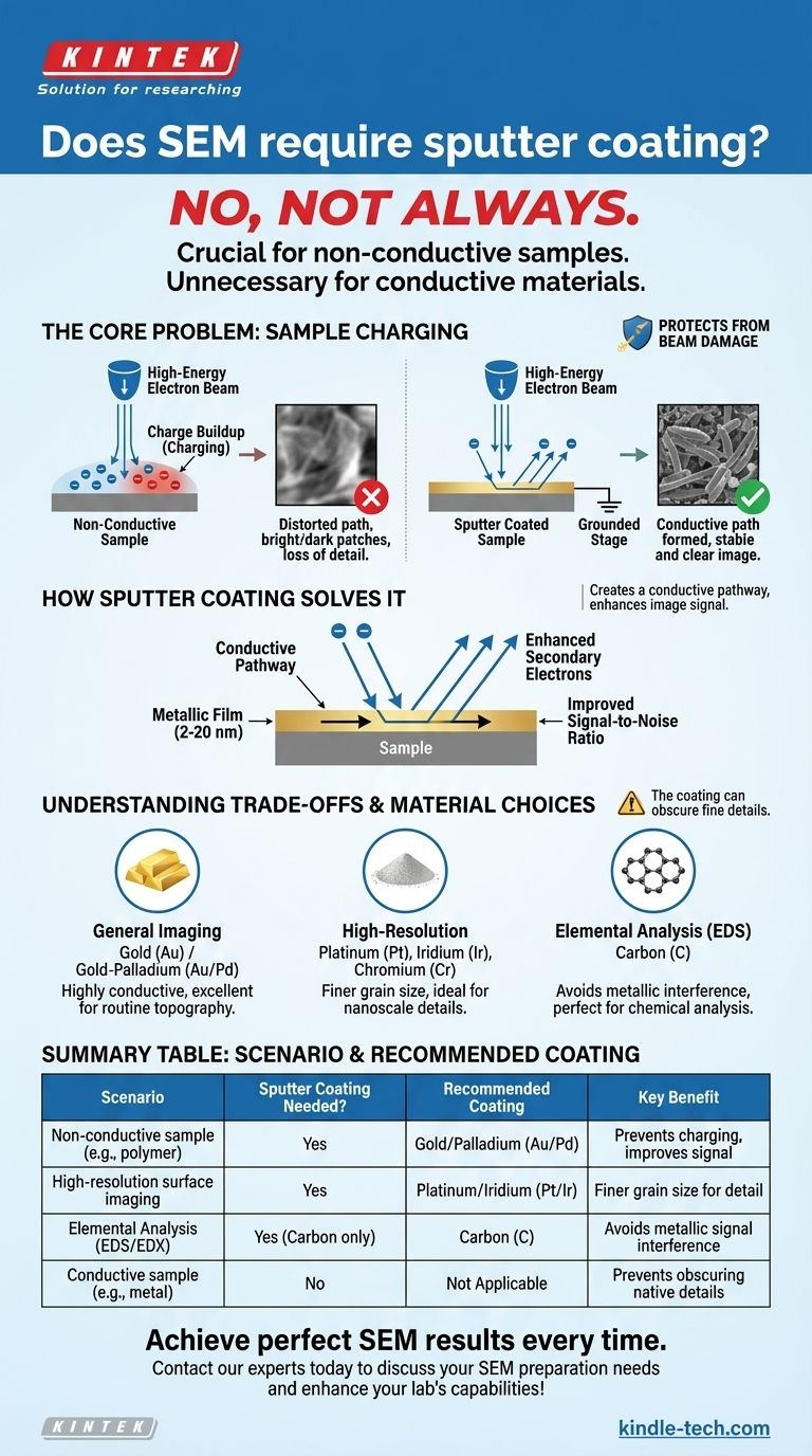
No, SEM does not always require sputter coating. It is a critical preparation technique specifically for samples that are non-conductive or poorly conductive. For materials that are already electrically conductive, such as metals, sputter coating is unnecessary and can even obscure important surface details.
The core purpose of an SEM is to read the story told by electrons interacting with a sample's surface. Sputter coating is the essential translation step that allows non-conductive materials—which would otherwise become a garbled mess of electrical charge—to tell their story clearly.

The Core Problem: Sample Charging
An SEM works by scanning a focused beam of high-energy electrons across a sample. To create an image, detectors measure the secondary electrons that are knocked off the sample's surface.
The Issue of "Charging"
When the sample is non-conductive (e.g., polymers, ceramics, biological tissue), the electrons from the beam have nowhere to go. They accumulate on the surface.
This buildup of negative charge, known as charging, severely distorts the electron beam's path. It results in bright patches, dark bands, and a complete loss of image detail, rendering the analysis useless.
The Challenge of Beam Damage
The intense electron beam can also deposit a significant amount of energy into the sample. For delicate, beam-sensitive materials, this can cause melting, cracking, or other forms of physical damage, destroying the very features you want to observe.
How Sputter Coating Solves the Problem
Sputter coating is the process of depositing an ultra-thin layer of conductive material, typically a metal, onto the sample's surface before it goes into the SEM.
Creating a Conductive Pathway
This metallic film, usually only 2 to 20 nanometers thick, forms a continuous conductive path. Electrons from the beam can now travel harmlessly along this coating to the grounded SEM sample stage instead of accumulating on the surface.
This immediately eliminates the problem of charging, allowing for a stable and clear image to be formed.
Enhancing Image Signal
The metals used for coating are excellent emitters of secondary electrons. This means that for every primary electron that hits the surface, more secondary electrons are generated than would be from the uncoated sample.
This process dramatically improves the signal-to-noise ratio, leading to a sharper, more detailed image of the sample's surface topography. The coating also acts as a protective barrier, absorbing some beam energy and protecting sensitive samples from damage.
Understanding the Trade-offs and Material Choices
While essential, sputter coating is not without its considerations. You are technically imaging the coating, not the native sample surface, which introduces important trade-offs.
The Coating Can Obscure Fine Details
The coating material itself has a structure, known as grain size. If you are trying to image nanoscale features that are smaller than the grain size of your coating, those features will be hidden. A thicker coating will obscure more detail.
Choosing the Right Material is Critical
The material you choose to coat with depends entirely on your analysis goal.
-
Gold (Au) or Gold/Palladium (Au/Pd): This is the most common choice for general-purpose imaging. Gold is highly conductive and easy to sputter, providing excellent results for routine topographic analysis.
-
Platinum (Pt), Iridium (Ir), Chromium (Cr): These materials have a much finer grain size than gold. They are the preferred choice for very high-magnification, high-resolution work where resolving the smallest possible surface features is critical.
-
Carbon (C): Carbon is used almost exclusively when performing Energy-Dispersive X-ray Spectroscopy (EDX/EDS). This technique identifies the elements within your sample. A metallic coating would produce strong X-ray signals that interfere with and obscure the signals from the actual sample. Carbon's low-energy X-ray peak does not conflict with most other elements, making it ideal for this type of chemical analysis.
Making the Right Choice for Your Sample
Your decision to use sputter coating—and which material to use—should be a direct function of your sample's properties and your analytical goal.
- If your primary focus is high-resolution surface topography: Use a fine-grained metal like platinum or iridium to resolve the smallest features.
- If your primary focus is elemental analysis (EDX/EDS): You must use carbon coating to avoid signal interference from a metallic coat.
- If your primary focus is general imaging of a non-conductor: Gold or a gold/palladium alloy is a reliable and cost-effective choice.
- If your sample is already conductive (e.g., a metal or alloy): Sputter coating is unnecessary and should be avoided.
Ultimately, understanding the interplay between your sample, your analysis goal, and the electron beam is the key to mastering SEM sample preparation.
Summary Table:
| Scenario | Sputter Coating Needed? | Recommended Coating | Key Benefit |
|---|---|---|---|
| Non-conductive sample (e.g., polymer, ceramic) | Yes | Gold/Palladium (Au/Pd) | Prevents charging, improves signal |
| High-resolution surface imaging | Yes | Platinum/Iridium (Pt/Ir) | Finer grain size for detail |
| Elemental Analysis (EDS/EDX) | Yes (Carbon only) | Carbon (C) | Avoids metallic signal interference |
| Conductive sample (e.g., metal) | No | Not Applicable | Prevents obscuring native details |
Achieve perfect SEM results every time. The right sample preparation is critical for clear, accurate imaging and analysis. KINTEK specializes in lab equipment and consumables, serving laboratory needs with reliable sputter coaters and expert advice. Let our team help you select the ideal coating strategy for your specific samples and analysis goals.
Contact our experts today to discuss your SEM preparation needs and enhance your lab's capabilities!
Visual Guide

Related Products
People Also Ask
- What is the difference between electrolyte and electrode cell? Master the Fundamentals of Electrochemical Systems
- What type of electrode system is the coating evaluation electrolytic cell designed for? Unlock Precise Coating Analysis
- What is the difference between a voltaic cell and an electrochemical cell? Understand the Two Types of Energy Conversion
- What is the procedure for starting the experiment and what should be observed? A Step-by-Step Guide for Reliable Electrochemistry
- How does a standardized electrochemical test cell assist in MOx/CNTf electrode screening? Optimize Material Ratios
