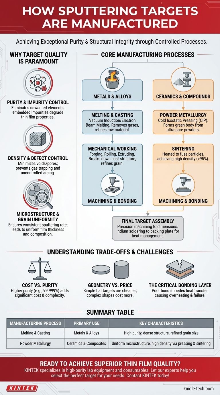
Sputtering targets are manufactured through a multi-step, highly controlled process designed to achieve exceptional purity and structural integrity. The primary methods involve either melting and casting for metallic targets or powder metallurgy techniques like pressing and sintering for ceramic and composite targets, followed by precision machining and bonding to a backing plate.
The core objective of sputtering target manufacturing is not simply to create a block of material, but to engineer a source with extreme purity, high density, and a uniform microstructure. These properties are critical because any imperfection in the target will be directly transferred into the thin film being deposited.
Why Target Quality is Paramount
The manufacturing process for a sputtering target is far more rigorous than for standard industrial materials. This is because the target serves as the source material for creating a thin film, and its characteristics directly dictate the performance and reliability of the final product.
Purity and Impurity Control
Impurities within the target material, such as unwanted elements or oxides, will be sputtered along with the desired material. These contaminants become embedded in the deposited film, which can severely degrade its electrical, optical, or mechanical properties.
Density and Defect Control
A sputtering target must be as close to its theoretical maximum density as possible. Voids, cracks, or pores within the material can trap gas, leading to uncontrolled arcing during the sputtering process. This arcing can damage the substrate and create defects in the film.
Microstructure and Grain Uniformity
The size and orientation of the crystalline grains within the target affect the sputtering rate. A uniform, fine-grained microstructure ensures a consistent and stable deposition process, leading to a film with uniform thickness and composition.
Core Manufacturing Processes
While specific steps vary based on the material, most manufacturing falls into two primary pathways followed by finishing and bonding.
For Metals and Alloys: Melting and Casting
This is the most common method for producing pure metal or alloy targets. The process typically involves vacuum induction melting or electron beam melting to refine the raw material and remove dissolved gasses and impurities.
The molten metal is then cast into an ingot, which is subsequently forged, rolled, or extruded. These mechanical working steps help to break down the cast structure, refine the grain size, and create a dense, uniform material ready for final machining.
For Ceramics and Compounds: Powder Metallurgy
Ceramic targets, such as Indium Tin Oxide (ITO) or Titanium Nitride (TiN), cannot be manufactured through melting. Instead, they are made by consolidating ultra-pure powders.
A common technique is Cold Isostatic Pressing (CIP), where the powder is placed in a flexible mold and subjected to extreme hydrostatic pressure. This forms a compacted preform, known as a "green body," which is then sintered (heated to a high temperature below its melting point) to fuse the particles together, achieving densities often exceeding 95% of the theoretical maximum.
Final Machining and Bonding
Regardless of the initial method, the consolidated material must be precisely machined to the exact dimensions required by the sputtering system, which can be flat, circular, or cylindrical.
Finally, the finished target material is bonded, typically using indium soldering, to a metallic backing plate. This backing plate provides structural support and integrates with the system's water-cooling channels to manage the intense heat generated during sputtering.
Understanding the Trade-offs and Challenges
Manufacturing a high-quality target involves balancing competing factors and overcoming significant technical hurdles.
Cost vs. Purity
Achieving higher levels of purity (e.g., 99.999%) requires additional refining steps, each adding significant cost and complexity to the process. For less critical applications, a lower-purity target may be a more economical choice.
Geometry vs. Price
Simple, flat targets are the easiest to manufacture and therefore the least expensive. More complex geometries, such as ring-shaped or cylindrical targets required by specific sputtering tools, involve more intricate machining and have a higher associated cost.
The Critical Bonding Layer
The bond between the target material and the backing plate is a common point of failure. A poor bond can impede heat transfer, causing the target to overheat, crack, or even de-laminate during the sputtering process, leading to catastrophic failure.
Making the Right Choice for Your Application
The ideal manufacturing process is dictated entirely by the requirements of the final thin film.
- If your primary focus is high-performance electronics: You must prioritize targets with the highest possible purity and density, typically made through advanced vacuum melting or hot isostatic pressing (HIP).
- If your primary focus is general protective coatings: Standard melting and casting or CIP processes often provide a sufficient balance of quality and cost-effectiveness for applications like tool coatings.
- If your primary focus is research and development: Your needs may require custom alloys or unique composites, favoring the flexibility of powder metallurgy and specialized hot-pressing techniques.
Ultimately, understanding how a sputtering target is made empowers you to select the right material source to control the quality and performance of your final product.
Summary Table:
| Manufacturing Process | Primary Use | Key Characteristics |
|---|---|---|
| Melting & Casting | Metals & Alloys | High purity, dense structure, refined grain size |
| Powder Metallurgy | Ceramics & Composites | Uniform microstructure, high density via pressing & sintering |
Ready to achieve superior thin film quality? The right sputtering target is critical for your application's success. KINTEK specializes in high-purity lab equipment and consumables, providing sputtering targets engineered for exceptional performance in electronics, protective coatings, and R&D. Let our experts help you select the perfect target for your needs. Contact KINTEK today to discuss your project!
Visual Guide
Related Products
- Reference Electrode Calomel Silver Chloride Mercury Sulfate for Laboratory Use
- Multifunctional Electrolytic Electrochemical Cell Water Bath Single Layer Double Layer
- Molybdenum Tungsten Tantalum Special Shape Evaporation Boat
- Hemispherical Bottom Tungsten Molybdenum Evaporation Boat
- Cylindrical Press Mold with Scale for Lab
People Also Ask
- What is the function of a reference electrode? Master Precision in Three-Electrode Reactor Reconstruction
- What is the reference electrode in potentiometry? The Key to Stable & Accurate Measurements
- Why is the selection of a high-quality reference electrode critical in the electrochemical synthesis? | KINTEK
- Which electrode is used as a reference electrode for measuring half-cell potentials? Understanding the Universal Standard
- How does the selection of reference electrodes correlate with electrolyte pH in HER testing? Ensure Precise Potential


