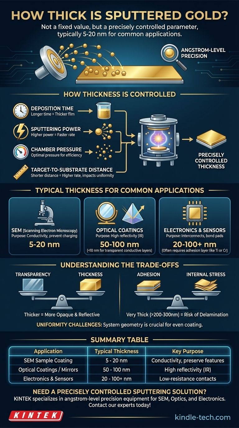
The thickness of a sputtered gold layer is not a fixed value but is a precisely controlled parameter of the deposition process. The thickness is determined by the specific requirements of the application. For many common uses, such as preparing samples for electron microscopy, this layer is typically between 5 and 20 nanometers (nm) thick.
The central concept to grasp is that you don't ask "how thick is sputtered gold," but rather "what thickness can I achieve with sputtering?" The process offers angstrom-level precision, allowing you to engineer a film perfectly tailored to a specific function, from nearly transparent conductive layers to fully opaque mirrors.
How Sputtering Thickness is Controlled
The final thickness of a sputtered film is a direct result of several key process parameters. The deposition rate, measured in angstroms or nanometers per second, is managed by the technician to achieve the target thickness with high precision.
The Role of Deposition Time
This is the most straightforward control variable. All other factors being equal, the longer the substrate is exposed to the flux of sputtered gold atoms, the thicker the resulting film will be. Automated systems can shut off the process after a pre-set time to achieve a specific thickness.
The Impact of Sputtering Power
The sputtering power, typically DC power for a conductive target like gold, dictates the energy of the ions bombarding the target. Higher power results in a more aggressive bombardment, ejecting more gold atoms per second and thus increasing the deposition rate.
The Influence of Chamber Pressure
Sputtering occurs in a vacuum chamber filled with a small amount of an inert gas, usually argon. The pressure of this gas affects the efficiency of the process. If the pressure is too high, the sputtered gold atoms will collide with too many gas atoms, scattering them and reducing the deposition rate on the substrate.
Target-to-Substrate Distance
The physical distance between the gold target and the substrate being coated is critical. A shorter distance generally leads to a higher deposition rate, as more of the ejected atoms will land on the substrate. However, this can sometimes come at the cost of film uniformity across the substrate's surface.
Typical Thickness for Common Applications
The "right" thickness is entirely dependent on the goal. What works for one application is completely unsuitable for another, highlighting the importance of process control.
Scanning Electron Microscopy (SEM)
For SEM, non-conductive samples must be coated to prevent the buildup of electrical charge from the electron beam. A gold or gold-palladium layer of 5-20 nm is standard. This is thick enough to provide excellent conductivity but thin enough that it doesn't obscure the fine nanoscale features of the sample's surface.
Optical Coatings
In optics, gold is prized for its high reflectivity, especially in the infrared (IR) spectrum. A layer of 50-100 nm is often used to create a highly reflective mirror. Conversely, extremely thin layers (<10 nm) can be partially transparent while still being conductive, a property used in some specialized optical filters and transparent electrodes.
Electronics and Sensors
In microelectronics, gold is used for bond pads, interconnects, and contact layers due to its conductivity and resistance to oxidation. Thickness here can range from 20 nm to over 100 nm, depending on the current-carrying requirements. A thin adhesion layer of titanium or chromium is almost always deposited first to ensure the gold sticks to the substrate (e.g., silicon or glass).
Understanding the Trade-offs
Choosing a thickness is an engineering decision that involves balancing competing properties. There is no single "best" thickness, only the most appropriate one for a given task.
Thickness vs. Transparency
This is the most direct trade-off. As a gold film gets thicker, it absorbs and reflects more light, becoming more opaque. A 5 nm film may appear as a faint, transparent tint, while a 50 nm film will be fully opaque and mirror-like.
Adhesion and Internal Stress
Depositing a very thick layer of gold (>200-300 nm) can introduce significant internal stress into the film. This stress can cause the layer to delaminate or peel off the substrate, especially if the initial surface adhesion is poor.
Uniformity Challenges
Achieving a perfectly uniform thickness is harder than it sounds, especially on large or complex-shaped substrates. The sputtering system's geometry, including the target size and substrate rotation, must be carefully designed to ensure an even coating from edge to edge.
Defining Your Thickness Requirement
To select the correct thickness, you must first define your primary objective.
- If your primary focus is sample coating for SEM: Aim for a 5-20 nm layer to ensure conductivity without hiding nanoscale surface features.
- If your primary focus is creating an optical mirror: A thickness of 50-100 nm will typically provide excellent reflectivity, especially for infrared light.
- If your primary focus is electrical conductivity for electronics: A layer of 20-100 nm usually provides low resistance, but you must factor in the need for an adhesion layer like titanium.
Ultimately, gold sputtering provides the control to deposit the precise thickness your application demands, transforming thickness from a simple measurement into a powerful engineering parameter.
Summary Table:
| Application | Typical Thickness Range | Key Purpose |
|---|---|---|
| SEM Sample Coating | 5 - 20 nm | Conductivity without obscuring features |
| Optical Coatings / Mirrors | 50 - 100 nm | High reflectivity, especially in IR |
| Electronics & Sensors | 20 - 100+ nm | Low-resistance interconnects & contacts |
Need a precisely controlled gold sputtering solution for your lab? At KINTEK, we specialize in lab equipment and consumables that deliver angstrom-level precision for applications ranging from SEM sample preparation to advanced optical coatings. Our expertise ensures you achieve the exact thickness, uniformity, and adhesion your research demands. Contact our experts today to discuss how we can tailor a sputtering process to your specific requirements!
Visual Guide
Related Products
- Electron Beam Evaporation Coating Gold Plating Tungsten Molybdenum Crucible for Evaporation
- High Purity Gold Platinum Copper Iron Metal Sheets
- Gold Electrochemical Sheet Electrode Gold Electrode
People Also Ask
- What is e-beam evaporation? Achieve High-Purity Thin Film Deposition for Your Lab
- What is the container that holds the metal source material called in e-beam evaporation? Ensure Purity and Quality in Your Thin-Film Deposition
- How is an electron beam evaporator cooled during deposition? Essential Thermal Management for Stable Processes
- What is the temperature of e-beam evaporation? Mastering the Two-Zone Thermal Process for Precision Films
- What is the process of e-beam coating? Achieve High-Purity, Precise Thin Films for Your Lab