In short, the source of sputtered material is a solid "target" that is physically bombarded by high-energy ions. These ions, typically generated from an inert gas like argon, act like microscopic sandblasters, knocking atoms loose from the target material. These dislodged atoms then travel through a vacuum and deposit as a thin film onto a nearby surface, known as the substrate.
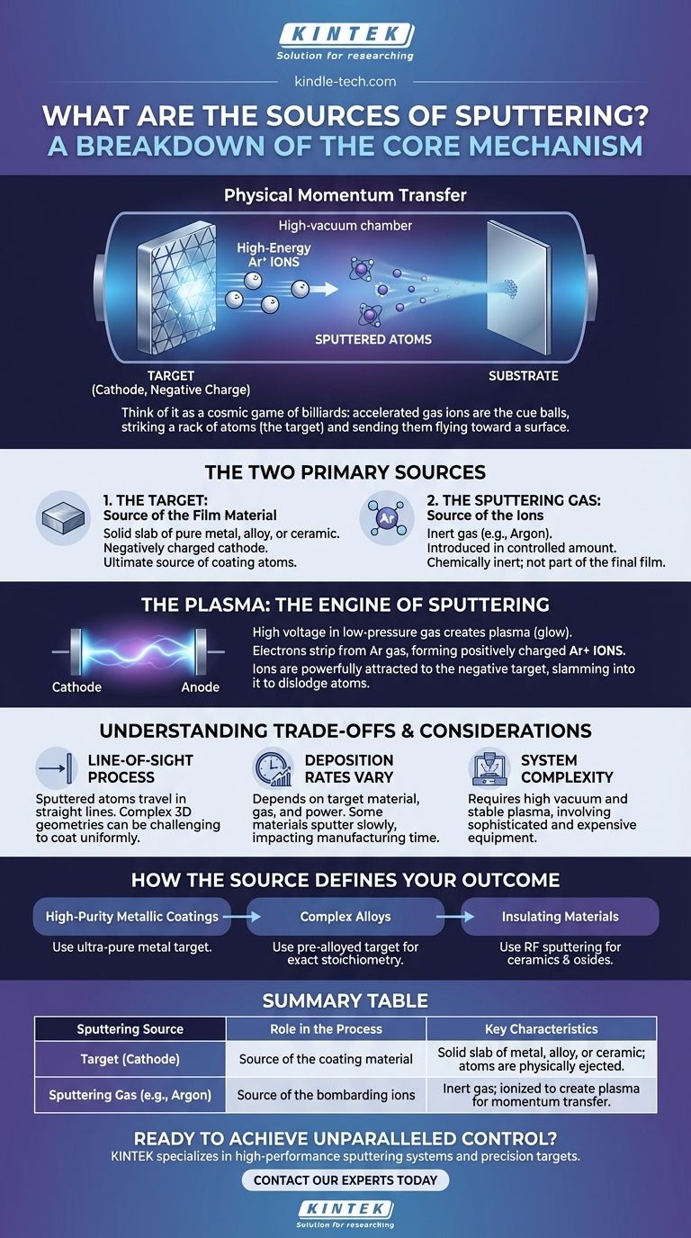
The sputtering process isn't a chemical reaction; it's a physical momentum transfer. Think of it as a cosmic game of billiards where accelerated gas ions are the cue balls, striking a rack of atoms (the target) and sending them flying toward a surface to form a perfectly uniform coating.
Sputtering: A Breakdown of the Core Mechanism
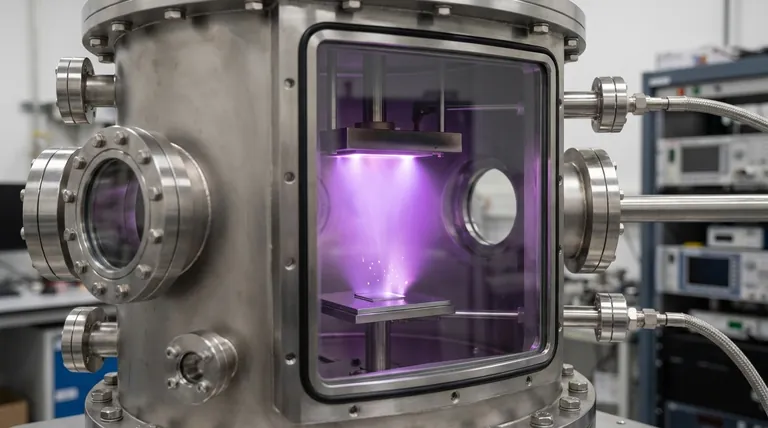
Sputtering is a highly controlled and versatile form of Physical Vapor Deposition (PVD). The entire process occurs within a high-vacuum chamber to ensure the purity and integrity of the resulting film.
The fundamental goal is to physically eject atoms from a source material and have them land precisely on a substrate. This is achieved by creating an energized environment where charged particles do the heavy lifting.
The Two Primary "Sources" in the Sputtering Process
To understand where the final film comes from, we need to look at two distinct but codependent sources: the source of the film material and the source of the energy that liberates it.
The Target: The Source of the Film Material
The target is a solid slab of the material you wish to deposit as a thin film. This is the ultimate source of the coating atoms.
This target can be a pure metal, an alloy, or even a ceramic compound. It is placed within the vacuum chamber and connected to a power supply that gives it a negative electrical charge, turning it into a cathode.
The Sputtering Gas: The Source of the Ions
An inert gas, most commonly Argon (Ar), is introduced into the vacuum chamber in a small, controlled amount. This gas is not part of the final film.
Its sole purpose is to be the source of the bombarding particles. It is chosen because it is heavy enough to dislodge target atoms effectively and is chemically inert, meaning it won't react with the target or the film.
The Plasma: The Engine of Sputtering
Applying a high voltage within the low-pressure gas environment creates a plasma, which is often visible as a characteristic glow.
In this plasma, electrons are stripped from the argon gas atoms, creating positively charged argon ions (Ar+). These positive ions are now strongly attracted to the negatively charged target.
The electric field accelerates these ions, causing them to slam into the target surface with significant force, dislodging or "sputtering" atoms from it.
Understanding the Trade-offs and Considerations
While sputtering is a powerful and precise technique, it's essential to understand its operational principles to recognize its limitations.
A Line-of-Sight Process
Sputtered atoms travel in a relatively straight line from the target to the substrate. While scattering in the gas provides some distribution, deeply recessed features or complex 3D geometries can be challenging to coat uniformly.
Deposition Rates Can Vary
The rate at which a film is deposited depends on the target material, the sputtering gas, and the power applied. Some materials sputter much more slowly than others, which can impact manufacturing time and cost.
System Complexity
Achieving the necessary high vacuum and generating a stable plasma requires sophisticated and expensive equipment. The process is not as simple as chemical dipping or electroplating.
How the Source Material Defines Your Outcome
The choice of target material and process parameters directly dictates the properties of your final thin film.
- If your primary focus is high-purity metallic coatings: Sputtering is ideal, as you can use an ultra-pure metal target to create a film with the same composition.
- If your primary focus is depositing complex alloys: You can use a pre-alloyed target to ensure the resulting film has the exact same stoichiometry as the source.
- If your primary focus is coating with insulating materials: Sputtering (specifically RF sputtering) is one of the few techniques that can effectively deposit high-quality films of materials like ceramics and oxides.
Ultimately, the sputtering process provides unparalleled control over film thickness, purity, and uniformity by precisely managing its sources.
Summary Table:
| Sputtering Source | Role in the Process | Key Characteristics |
|---|---|---|
| Target (Cathode) | Source of the coating material | Solid slab of metal, alloy, or ceramic; atoms are physically ejected. |
| Sputtering Gas (e.g., Argon) | Source of the bombarding ions | Inert gas; ionized to create plasma for momentum transfer. |
Ready to achieve unparalleled control over your thin film deposition?
KINTEK specializes in high-performance lab equipment, including sputtering systems and consumables like precision targets. Whether your focus is on high-purity metallic coatings, complex alloys, or insulating ceramics, our solutions are designed to meet the exacting demands of your laboratory.
Contact our experts today via our Contact Form to discuss how we can enhance your research and development with reliable, high-quality sputtering technology.
Visual Guide
Related Products
- Reference Electrode Calomel Silver Chloride Mercury Sulfate for Laboratory Use
- Multifunctional Electrolytic Electrochemical Cell Water Bath Single Layer Double Layer
- Molybdenum Tungsten Tantalum Special Shape Evaporation Boat
- Hemispherical Bottom Tungsten Molybdenum Evaporation Boat
- Cylindrical Press Mold with Scale for Lab
People Also Ask
- How does the selection of reference electrodes correlate with electrolyte pH in HER testing? Ensure Precise Potential
- Which type of electrode can be used as a reference point? Select the Right One for Accurate Measurements
- What is the purpose of the reference electrode? Achieve Stable & Accurate Electrochemical Measurements
- Which electrode is used as a reference? A Guide to Accurate Electrochemical Measurements
- Which electrode is used as a reference electrode for measuring half-cell potentials? Understanding the Universal Standard


