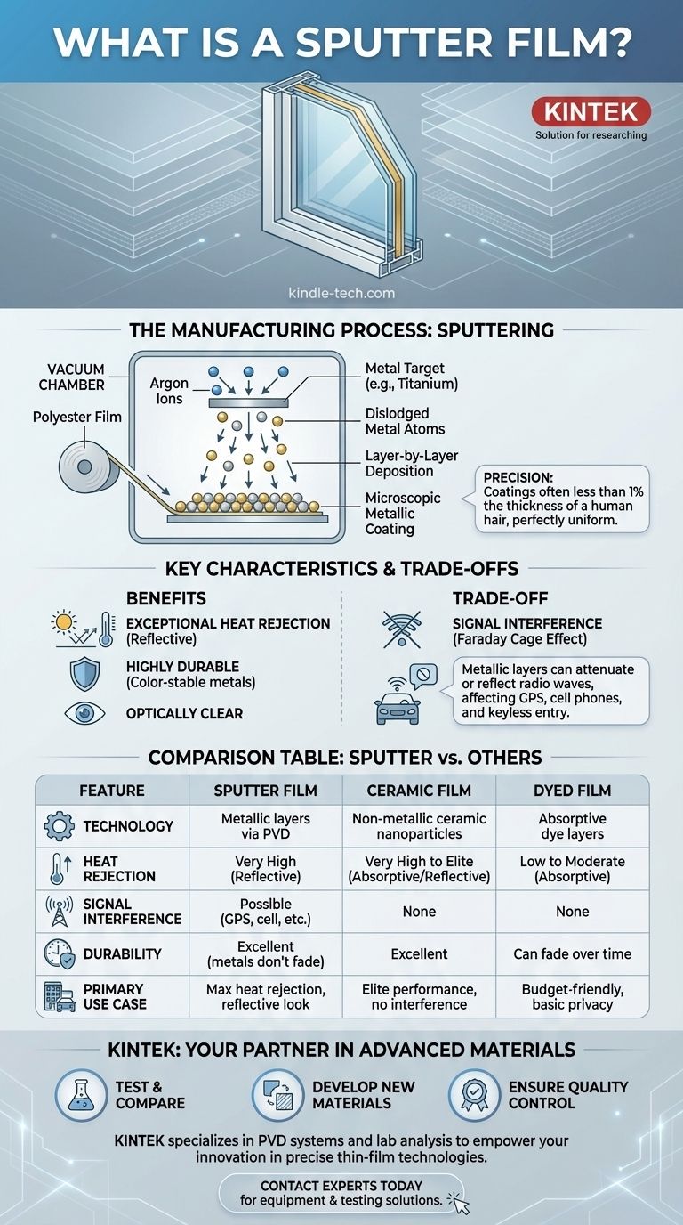
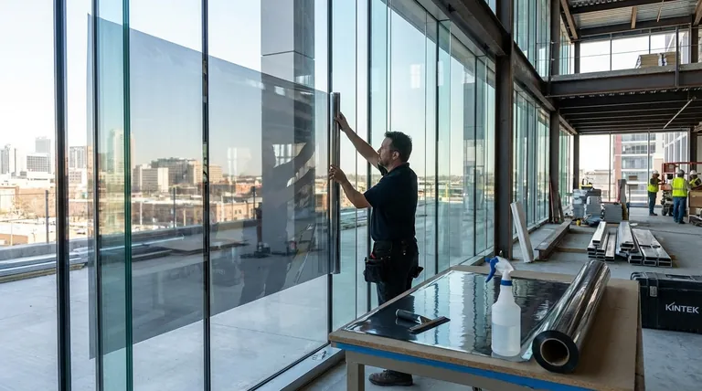
In the world of advanced materials, a sputter film is a high-performance window tint manufactured through a process called sputtering. In this high-tech method, a sheet of clear polyester film is placed in a vacuum chamber, where it is coated with microscopic, atomic layers of durable metals like titanium, stainless steel, gold, or silver. This process creates a film that is exceptionally effective at rejecting solar heat, highly durable, and optically clear.
Sputter film is defined by its manufacturing process: using ionized gas to bombard metals and deposit a thin, precise metallic coating onto film. While this provides outstanding heat rejection, its metallic nature creates a critical trade-off—potential interference with electronic signals—which has led to the rise of non-metallic ceramic films.
How Sputter Film is Made
The term "sputtering" refers to a physical vapor deposition (PVD) process. It is a precise, high-energy method that gives the film its unique performance characteristics.
The Vacuum Chamber Environment
The entire process takes place in a sealed, low-pressure vacuum chamber. This is critical to prevent the metals from reacting with oxygen or other particles in the air, ensuring a pure and optically perfect coating.
Atomic "Bombardment"
Inside the chamber, a target made of the desired metal (e.g., titanium) is bombarded with energized ions from an inert gas, such as argon. Think of it as a microscopic sandblaster, where ions chip away individual atoms from the metal target.
Layer-by-Layer Deposition
These dislodged metal atoms travel through the vacuum and deposit onto the cool surface of the polyester film. This builds up a coating that is incredibly thin—often less than 1% the thickness of a human hair—but perfectly uniform.
Building a Multi-Layered Structure
The true innovation of sputtering is the ability to create a stack of many different layers. By using multiple targets of different metals, manufacturers can fine-tune the film’s properties, controlling its color, reflectivity, and ability to block specific wavelengths of light like infrared (heat) and ultraviolet (UV).
Sputter Film vs. Other Window Tints
Understanding sputter film requires comparing it to the other common technologies on the market.
Compared to Dyed Film
Dyed films use simple dye layers that absorb solar energy, causing the glass to heat up. Sputter films use metallic layers to reflect solar energy, which is a more effective way to keep an interior cool. Furthermore, dyes fade over time and can turn purple, while the metals in sputter film are perfectly color-stable.
Compared to Carbon Film
Carbon film uses carbon particles to absorb and reflect heat. Its primary advantage is that it's non-metallic, so it doesn't interfere with electronic signals. While it offers good performance, high-end sputter films can often achieve slightly higher levels of heat rejection.
Compared to Ceramic Film
Ceramic film is the most modern competitor to sputter film. It uses non-conductive, non-metallic ceramic nanoparticles to block heat. Ceramic films can match or even exceed the heat rejection of sputter films without the risk of signal interference, making them the current state-of-the-art for high-performance applications.
Understanding the Trade-offs: The Signal Interference Problem
The greatest strength of sputter film—its metallic composition—is also its most significant weakness.
How Metals Block Radio Waves
The microscopic layers of metal in a sputter film can act as a weak shield against electromagnetic radiation. This is similar to the principle of a Faraday cage, which uses a metallic screen to block radio signals.
The Real-World Impact
This shielding effect can attenuate or reflect radio waves, potentially weakening the reception for GPS navigation, cell phones, satellite radio, and keyless entry systems. The degree of interference depends on the specific metals used and the density of the coating.
The Rise of Ceramic Technology
Ceramic window films were developed specifically to solve this problem. They provide elite heat rejection using advanced, non-metallic particles, ensuring zero impact on electronic communications.
Making the Right Choice for Your Goal
Choosing a window film depends entirely on balancing performance, aesthetics, and potential drawbacks for your specific application.
- If your primary focus is maximum heat rejection with a unique, reflective look: Sputter film remains an excellent choice, provided you understand and accept the potential for minor electronic signal interference.
- If your primary focus is elite heat rejection with zero risk of signal interference: Modern ceramic film is the superior and recommended technology for cars, modern homes, and commercial buildings.
- If your primary focus is affordability for basic privacy and moderate heat absorption: A quality dyed or carbon film will be the most cost-effective solution.
Ultimately, understanding the technology behind the film empowers you to select a solution that perfectly aligns with your priorities.
Summary Table:
| Feature | Sputter Film | Ceramic Film | Dyed Film |
|---|---|---|---|
| Technology | Metallic layers via PVD | Non-metallic ceramic nanoparticles | Absorptive dye layers |
| Heat Rejection | Very High (Reflective) | Very High to Elite (Absorptive/Reflective) | Low to Moderate (Absorptive) |
| Signal Interference | Possible (GPS, cell, etc.) | None | None |
| Durability/Color Stability | Excellent (metals don't fade) | Excellent | Can fade over time |
| Primary Use Case | Max heat rejection, reflective look | Elite performance, no interference | Budget-friendly, basic privacy/heat reduction |
Need a High-Performance Solution for Your Project?
Whether you're specifying materials for automotive, architectural, or specialized glazing applications, understanding the properties of coatings like sputter film is crucial. At KINTEK, we specialize in the advanced equipment and consumables needed for developing and testing these precise thin-film technologies.
Our expertise in PVD systems and lab analysis can help you:
- Test and compare the performance of different film types.
- Develop new materials with specific optical and thermal properties.
- Ensure quality control for consistent, high-performance results.
Let KINTEK's laboratory equipment solutions empower your innovation. Contact our experts today to discuss how we can support your specific needs in advanced materials and coating technologies.
Visual Guide