At its core, plasma sputtering is a physical process of atomic-scale billiards. In a high-vacuum chamber, energized ions are accelerated to strike a solid source material, known as the "target." This collision has enough force to physically knock out, or "sputter," individual atoms from the target, which then travel and deposit onto a substrate, building a highly uniform and controlled thin film.
Sputtering is not merely a coating method; it is a precision engineering technique. Its value lies in the exceptional control it offers over a film's thickness, density, and structure at the atomic level, making it indispensable for high-performance applications.

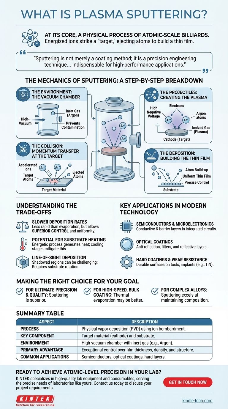
The Mechanics of Sputtering: A Step-by-Step Breakdown
To understand sputtering, it's best to visualize the process as a sequence of events occurring within a specialized vacuum environment. Each step is critical for achieving the final desired film properties.
The Environment: The Vacuum Chamber
The entire process takes place inside a high-vacuum chamber. This serves two purposes: it prevents airborne particles from contaminating the film and allows the sputtered atoms to travel from the target to the substrate without colliding with other gas molecules.
Once a vacuum is established, a small amount of an inert gas, almost always Argon, is introduced.
The Projectiles: Creating the Plasma
A high negative voltage is applied to the target material, which acts as the cathode. This strong electric field energizes free electrons in the chamber.
These energetic electrons collide with the neutral Argon atoms, knocking an electron off and creating positively charged Argon ions (Ar+). This cloud of ionized gas is the plasma.
The Collision: Momentum Transfer at the Target
The positively charged Argon ions are forcefully accelerated toward the negatively charged target. They strike the target's surface with significant kinetic energy.
This impact transfers momentum from the ion to the target atoms, much like a cue ball striking a rack in billiards. If the energy transfer is sufficient, it ejects atoms from the target surface.
The Deposition: Building the Thin Film
The ejected, or sputtered, atoms of the target material travel through the vacuum chamber. They eventually strike the substrate—the component being coated—and stick to its surface.
Over time, millions of these atoms build up, layer by layer, to form a thin, dense, and highly uniform film. The thickness can be controlled with extreme precision, from a few nanometers to several micrometers.
Understanding the Trade-offs
Like any technical process, sputtering involves a series of trade-offs that make it more suitable for some applications than others. Objectively weighing these factors is key to making the right choice.
Slower Deposition Rates
Compared to other methods like thermal evaporation, sputtering is generally a slower process. The atom-by-atom ejection is inherently less rapid than boiling a material.
However, this slowness is directly linked to its greatest strength: control. The slower rate allows for the formation of denser, more uniform films with superior adhesion and microstructure.
Potential for Substrate Heating
The energetic bombardment and plasma processes can transfer a significant amount of heat to the substrate. This can be a concern when coating temperature-sensitive materials like plastics.
Advanced sputtering systems use cooling stages for the substrate to mitigate this effect, but it remains a critical process parameter to monitor and control.
Line-of-Sight Deposition
Sputtered atoms travel in a generally straight line from the target to the substrate. This can make it challenging to uniformly coat complex, three-dimensional shapes with shadowed regions.
Techniques like substrate rotation and planetary motion are employed to overcome this limitation and ensure even coverage on non-flat surfaces.
Key Applications in Modern Technology
Sputtering's precision has made it a cornerstone process in manufacturing the most advanced products we use every day.
Semiconductors and Microelectronics
Sputtering is used to deposit the conductive metal layers (interconnects) and barrier layers within integrated circuits. Its ability to create pure, thin, and uniform films is essential for reliable chip performance.
Optical Coatings
The process is ideal for creating anti-reflection coatings on lenses, filters for specific wavelengths of light, and reflective layers on mirrors and CDs. The precise control over film thickness directly relates to its optical properties.
Hard Coatings and Wear Resistance
Materials like Titanium Nitride (TiN) can be sputtered onto machine tools, drill bits, and medical implants. This creates an extremely hard, wear-resistant surface that dramatically extends the component's lifespan.
Making the Right Choice for Your Goal
Selecting a deposition method depends entirely on your project's primary objective.
- If your primary focus is ultimate precision and film quality: Sputtering is the superior choice for creating dense, uniform, and adherent films with controlled structure.
- If your primary focus is high-speed, bulk coating of simple materials: Thermal evaporation may be a more cost-effective and faster alternative.
- If you are working with complex alloys or compounds: Sputtering excels at maintaining the original material's composition (stoichiometry) in the final film.
Ultimately, choosing plasma sputtering is a decision to prioritize atomic-level control over raw deposition speed.
Summary Table:
| Aspect | Description |
|---|---|
| Process | Physical vapor deposition (PVD) using ion bombardment. |
| Key Component | Target material (cathode) and substrate. |
| Environment | High-vacuum chamber with inert gas (e.g., Argon). |
| Primary Advantage | Exceptional control over film thickness, density, and structure. |
| Common Applications | Semiconductors, optical coatings, and hard, wear-resistant layers. |
Ready to Achieve Atomic-Level Precision in Your Lab?
Plasma sputtering is the key to creating high-performance thin films with superior uniformity and adhesion. Whether you are developing next-generation semiconductors, advanced optical coatings, or durable wear-resistant surfaces, the right equipment is critical for success.
KINTEK specializes in high-quality lab equipment and consumables, serving the precise needs of laboratories like yours. Our expertise can help you select the ideal sputtering system to meet your specific research and production goals, ensuring reliability and repeatability in your results.
Contact us today to discuss your project requirements and discover how our solutions can enhance your capabilities.
Visual Guide
Related Products
- Spark Plasma Sintering Furnace SPS Furnace
- Chemical Vapor Deposition CVD Equipment System Chamber Slide PECVD Tube Furnace with Liquid Gasifier PECVD Machine
- RF PECVD System Radio Frequency Plasma-Enhanced Chemical Vapor Deposition RF PECVD
- Microwave Plasma Chemical Vapor Deposition MPCVD Machine System Reactor for Lab and Diamond Growth
- 915MHz MPCVD Diamond Machine Microwave Plasma Chemical Vapor Deposition System Reactor
People Also Ask
- What is the pressure for spark plasma sintering? A Guide to Optimizing SPS Parameters
- What is SPS sintering method? A Guide to High-Speed, High-Performance Material Fabrication
- What technical advantages does a Spark Plasma Sintering (SPS) furnace offer for LZP ceramics? Enhance Ionic Conductivity
- What are the fundamentals of spark plasma sintering process? Unlock Rapid, High-Performance Material Consolidation
- What are the advantages of CAMI/SPS for W-Cu composite preparation? Reduce cycles from hours to seconds.


