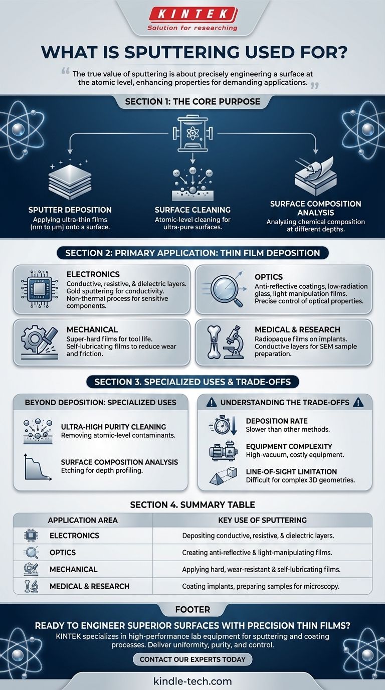
At its core, sputtering is a highly controlled process used for three main purposes. The most common is sputter deposition, an advanced technique for applying ultra-thin films of material onto a surface. It is also used in specialized cases for cleaning surfaces at an atomic level and for analyzing the chemical composition of a material. This technology is fundamental to manufacturing countless high-tech products, from semiconductors and disk drives to optical lenses and medical implants.
The true value of sputtering isn't just coating an object; it's about precisely engineering a surface at the atomic level. By depositing ultra-thin, highly uniform films, this technique fundamentally changes a material's properties—enhancing its conductivity, durability, or optical characteristics for demanding applications.
The Primary Application: Thin Film Deposition
The vast majority of sputtering applications involve depositing a thin film, ranging from a few nanometers to several micrometers thick, onto a substrate within a high-vacuum chamber. This precision allows for the creation of components with highly specialized surface properties.
Engineering High-Performance Electronics
Sputtering is a cornerstone of the microelectronics and semiconductor industries. It is a non-thermal coating technology, making it ideal for sensitive components.
Manufacturers use sputtering to lay down the microscopic layers of conductive, resistive, and dielectric materials needed to build integrated circuits. Gold sputtering, for example, is used for its excellent conductivity on circuit panels and electronic components.
Advancing Optical Technologies
The technique is critical for producing functional films with specific optical properties. This allows for precise control over how a surface interacts with light.
Applications include creating anti-reflective coatings on lenses, producing low-radiation glass for energy-efficient windows, and depositing films that absorb, transmit, or polarize light for specialized optical devices.
Enhancing Mechanical Durability
In the machining and manufacturing industries, sputtering is used to create surface functional films that improve a product's physical resilience.
This includes applying super-hard films to cutting tools to extend their life and depositing self-lubricating films on moving parts to reduce wear and friction.
Supporting Medical and Scientific Research
Sputtering plays a vital role in both medicine and fundamental science. Its precision and material compatibility are essential for sensitive applications.
In medicine, gold sputtering is used to coat biomedical implants with radiopaque films, making them visible in X-rays. In life sciences, it's used to apply an ultra-thin conductive gold layer to non-conductive tissue samples, making them visible under an electron microscope.
Beyond Deposition: Specialized Uses
While deposition is its most common function, the underlying physical process of sputtering is also leveraged for other high-purity tasks.
Ultra-High Purity Surface Cleaning
The same mechanism that ejects atoms from a target material for deposition can be used to meticulously clean a substrate.
By bombarding a surface with ions, sputtering can remove atomic-level contaminants, preparing an ultra-pure surface for research or subsequent processing steps.
Surface Composition Analysis
Sputtering can be used as a method for etching away a material, layer by layer.
When combined with other analytical techniques, this allows scientists to determine the chemical composition of a material at different depths from the surface.
Understanding the Trade-offs
Sputtering is a powerful and precise technique, but it is not the solution for every application. Understanding its limitations is key to using it effectively.
Deposition Rate
Sputtering is a highly controlled process, which often means it has a slower deposition rate compared to other coating methods like chemical vapor deposition or electroplating.
Equipment Complexity
The process requires a high-vacuum environment. The vacuum chambers and associated equipment are complex, require significant investment, and have high operating costs.
Line-of-Sight Limitation
In most sputtering configurations, the deposited material travels in a straight line from the target to the substrate. This can make it difficult to achieve a uniform coating on objects with complex, three-dimensional geometries.
Matching the Technique to the Goal
To determine if sputtering is the right choice, consider your primary objective.
- If your primary focus is precision electronics: Sputtering is the industry standard for creating the highly uniform conductive and resistive thin films required for integrated circuits.
- If your primary focus is advanced optics: This technique offers unparalleled control for depositing films that manipulate the reflection, transmission, or polarization of light.
- If your primary focus is mechanical performance: Sputtering is an excellent choice for applying extremely hard or self-lubricating coatings that significantly enhance component durability.
- If your primary focus is scientific analysis or medical devices: The technique provides the high-purity, biocompatible, and precise coatings necessary for research and sensitive implant applications.
Ultimately, sputtering empowers us to dictate the properties of a material's surface, turning ordinary substrates into highly specialized components.
Summary Table:
| Application Area | Key Use of Sputtering |
|---|---|
| Electronics | Depositing conductive, resistive, and dielectric layers for integrated circuits and components. |
| Optics | Creating anti-reflective coatings, low-radiation glass, and light-manipulating films. |
| Mechanical | Applying hard, wear-resistant coatings to cutting tools and self-lubricating films. |
| Medical & Research | Coating biomedical implants and preparing non-conductive samples for electron microscopy. |
Ready to engineer superior surfaces with precision thin films?
KINTEK specializes in high-performance lab equipment and consumables for sputtering and other advanced coating processes. Whether you are developing next-generation semiconductors, durable medical devices, or specialized optical components, our solutions deliver the uniformity, purity, and control your R&D or production demands.
Contact our experts today to discuss how we can support your specific laboratory needs.
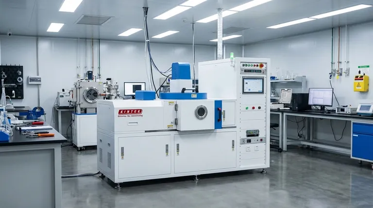
Visual Guide
Related Products
- Spark Plasma Sintering Furnace SPS Furnace
- Lab Sterile Slapping Type Homogenizer for Tissue Mashing and Dispersing
People Also Ask
- What is the difference between spark plasma sintering and flash sintering? A Guide to Advanced Sintering Methods
- What technical advantages does a Spark Plasma Sintering (SPS) furnace offer for LZP ceramics? Enhance Ionic Conductivity
- What is the process fundamentals of spark plasma sintering? Achieve Rapid, High-Density Material Consolidation
- Why are Spark Plasma Sintering (SPS) furnaces or hot presses utilized in the preparation of Li3PS4 solid electrolytes?
- What are the fundamentals of spark plasma sintering process? Unlock Rapid, High-Performance Material Consolidation

