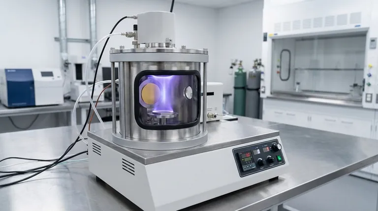
At its core, the function of a sputter coater is to deposit an exceptionally thin and uniform layer of material, often a metal, onto the surface of a sample. It accomplishes this through a physical process where high-energy ions bombard a source material (the target), dislodging atoms that then travel and coat the sample (the substrate). This technique is fundamental for preparing non-conductive samples for analysis in a scanning electron microscope (SEM) and for fabricating thin films in microelectronics and optics.
Sputter coating is a vacuum deposition technique that uses an energized plasma to physically eject atoms from a source material. This "atomic sandblasting" process allows you to create highly uniform, ultra-thin films with precise control over their thickness and composition.
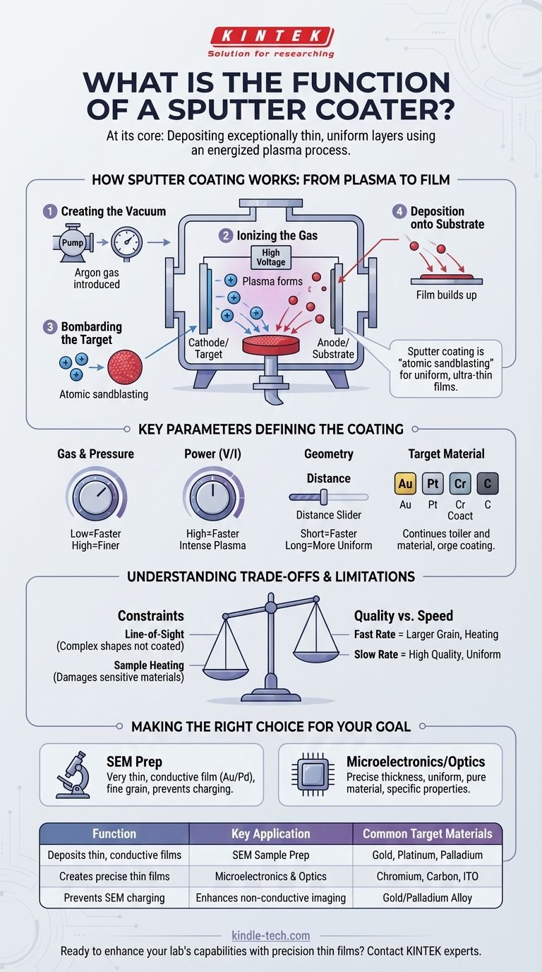
How Sputter Coating Works: From Plasma to Film
The process takes place within a vacuum chamber and relies on a sequence of controlled physical events to build the coating atom by atom.
Creating the Plasma Environment
First, the sample chamber is pumped down to a low pressure, creating a vacuum. An inert gas, most commonly argon, is then introduced into the chamber. This controlled, low-pressure gas environment is essential for the next steps.
Ionizing the Gas
A high voltage is applied between two electrodes: the cathode (which is the target material you want to deposit, like gold or platinum) and the anode (where the sample or substrate is placed). This strong electric field energizes the argon gas, stripping electrons from the argon atoms and creating a plasma—a glowing mixture of positively charged argon ions and free electrons.
Bombarding the Target
The positively charged argon ions are forcefully accelerated by the electric field and crash into the negatively charged target material. This energetic ion bombardment acts like a microscopic sandblaster, knocking individual atoms or small clusters of atoms free from the target surface. This ejection process is the "sputtering" itself.
Deposition onto the Substrate
The ejected target atoms travel in straight lines through the low-pressure chamber until they strike a surface. When they land on your sample, they condense and gradually build up to form a thin, continuous film. The result is a highly uniform coating that conforms to the sample's surface topography.
The Key Parameters That Define Your Coating
The quality, thickness, and deposition rate of the sputtered film are not accidental. They are directly controlled by several key process parameters.
The Role of Gas and Pressure
The pressure of the inert gas inside the chamber is critical. A higher pressure leads to more collisions and a slower, less direct path for the sputtered atoms, which can result in a finer-grained but less dense film. Lower pressure allows atoms to travel more directly, often increasing the deposition rate.
The Impact of Power (Voltage and Current)
The amount of electrical power applied to the target directly influences the deposition rate. Higher power (higher voltage or current) creates a more intense plasma, leading to more aggressive ion bombardment and a faster coating process.
The Importance of Geometry
The distance between the target and your sample plays a significant role. A shorter distance generally increases the deposition rate but may compromise the uniformity of the coating across a larger sample.
The Choice of Target Material
The material of the target itself dictates the properties of the final film. Gold, platinum, chromium, and carbon are common choices, each selected for specific properties like electrical conductivity, grain size, or resistance to oxidation.
Understanding the Trade-offs and Limitations
While powerful, sputter coating is not without its constraints. Understanding these trade-offs is crucial for achieving reliable and meaningful results.
It's a Line-of-Sight Process
Sputtered atoms travel in relatively straight lines. This means the process is "line-of-sight," and it cannot effectively coat deep trenches, undercuts, or the backside of a complex object. Areas not directly facing the target will receive little to no coating.
Potential for Sample Heating
The bombardment of sputtered atoms and other energetic particles from the plasma transfers energy to the sample, causing it to heat up. This can be a significant problem for heat-sensitive materials, such as biological specimens or polymers, potentially damaging or altering their structure.
Deposition Rate vs. Quality
Pushing for a very fast deposition rate by increasing power can be detrimental. It can lead to larger grain sizes in the film, which might obscure fine details on a sample for SEM imaging. It can also increase sample heating. A slower, more controlled deposition often yields a higher-quality, more uniform film.
Making the Right Choice for Your Goal
Your application determines how you should approach the sputter coating process.
- If your primary focus is SEM sample preparation: Your goal is a very thin, conductive coating (e.g., 5-10 nm of gold/palladium) that prevents electron charging without hiding the sample's surface features. Prioritize a fine-grained film over speed.
- If your primary focus is microelectronics or optical films: Your goal is precise control over film thickness, uniformity, and material purity. This requires careful calibration of all parameters—power, pressure, and time—to create a film with specific electrical or optical properties.
By understanding the fundamental principles of the process, you gain the ability to precisely control the outcome and generate thin films perfectly suited to your analytical or fabrication needs.
Summary Table:
| Function | Key Application | Common Target Materials |
|---|---|---|
| Deposits thin, uniform conductive films | SEM sample preparation | Gold, Platinum, Palladium |
| Creates precise thin films | Microelectronics & optics fabrication | Chromium, Carbon, ITO |
| Prevents sample charging in SEM | Enhances imaging of non-conductive samples | Gold/Palladium alloy |
Ready to enhance your lab's capabilities with precision thin films? KINTEK specializes in high-quality sputter coaters and lab equipment designed to meet the demanding needs of research and industrial laboratories. Whether you are preparing samples for SEM analysis or fabricating advanced microelectronic components, our solutions deliver the uniformity, control, and reliability you require. Contact our experts today to find the perfect sputter coater for your application!
Visual Guide
Related Products
- Custom CVD Diamond Coating for Lab Applications
- HFCVD Machine System Equipment for Drawing Die Nano-Diamond Coating
- Chemical Vapor Deposition CVD Equipment System Chamber Slide PECVD Tube Furnace with Liquid Gasifier PECVD Machine
- Multifunctional Electrolytic Electrochemical Cell Water Bath Single Layer Double Layer
- Professional Cutting Tools for Carbon Paper Cloth Diaphragm Copper Aluminum Foil and More
People Also Ask
- Can you coat something in diamond? Unlock Unmatched Hardness and Thermal Conductivity
- What are the different CVD coating? A Guide to Thermal CVD, PECVD, and Specialized Methods
- What is CVD diamond coating? Grow a Super-Hard, High-Performance Diamond Layer
- What is CVD coating? Transform Your Material's Surface for Maximum Performance
- What is CVD coating used for? Hardening Tools & Building Semiconductors for Industry


