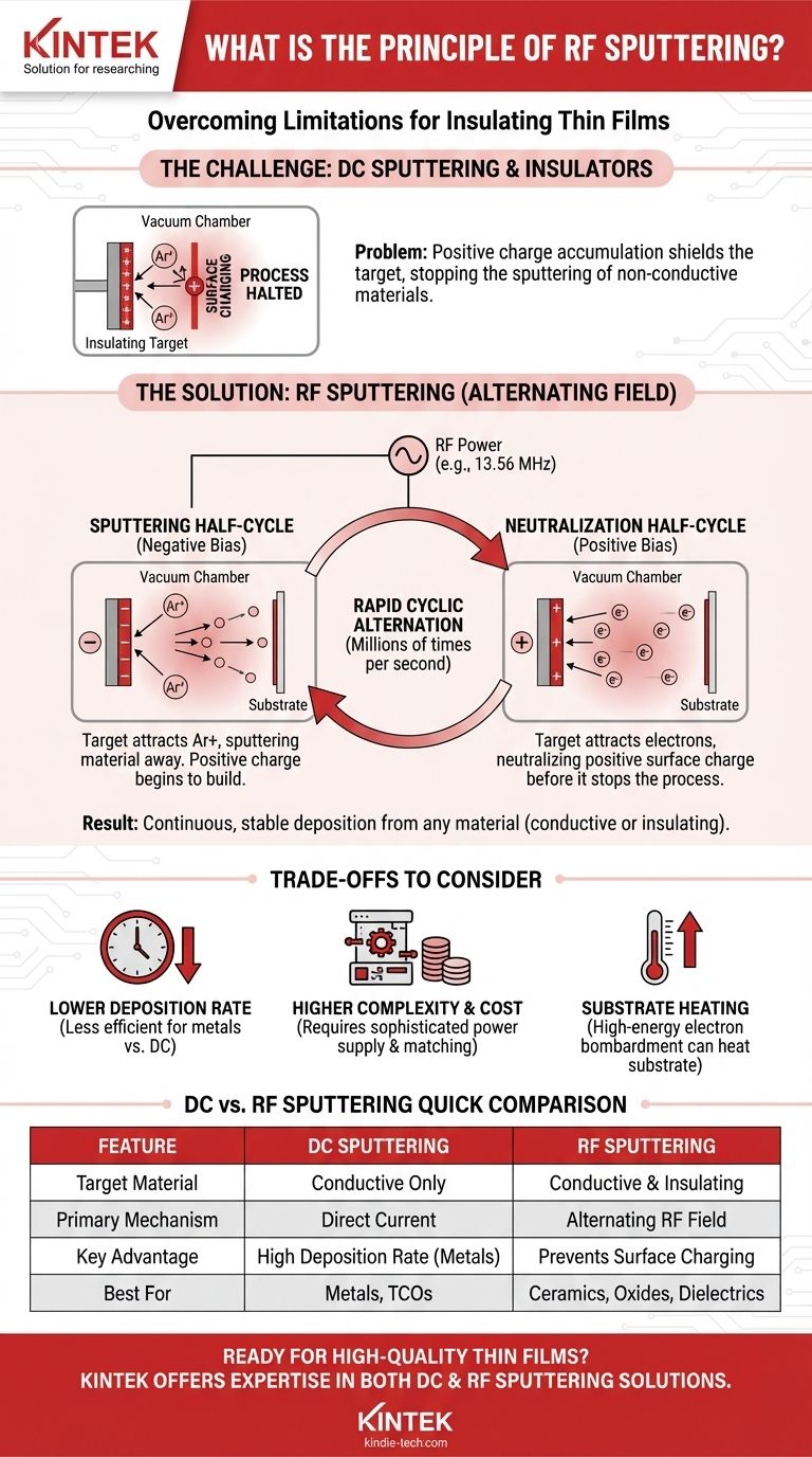
In principle, RF sputtering is a thin-film deposition technique that uses an alternating, radio-frequency electric field to create a plasma. This AC field overcomes the primary limitation of standard DC sputtering, allowing for the consistent deposition of thin films from electrically insulating (dielectric) materials, not just conductive ones. It achieves this by cyclically neutralizing charge build-up on the target's surface.
The core problem with sputtering insulating materials is that they accumulate a positive surface charge that repels the very ions needed for deposition. RF sputtering solves this by rapidly alternating the electric field, using one part of the cycle to sputter and the other to attract electrons that neutralize this charge.
The Foundation: How Basic Sputtering Works
To understand the innovation of RF sputtering, you must first grasp the principle of sputtering in general. It is a physical vapor deposition (PVD) process that occurs inside a vacuum chamber.
Creating the Plasma Environment
The process begins by introducing an inert gas, typically Argon, into a low-pressure vacuum chamber. An electric field is then applied, which energizes the gas and strips electrons from the Argon atoms, creating a glowing, ionized gas known as plasma.
The Bombardment Process
This plasma consists of positive Argon ions (Ar+) and free electrons. A target, made of the material you wish to deposit, is given a strong negative electrical potential, causing it to act as a cathode. The positive Argon ions are accelerated by this field and bombard the surface of the target at high energy.
Ejection and Deposition
The force of these ion impacts is strong enough to knock out, or "sputter," individual atoms from the target material. These ejected atoms travel through the vacuum chamber and condense as a uniform thin film on a substrate (like a silicon wafer) placed nearby.
The Challenge with Insulating Materials
The basic sputtering method described above is known as DC sputtering, as it uses a direct current power supply. It is highly effective for conductive materials but fails completely for insulators.
The Failure of DC Sputtering
When using a DC source with a non-conductive target (like a ceramic or an oxide), the process quickly stops. The target material, being an insulator, cannot dissipate the electrical charge from the constant stream of positive Argon ions bombarding its surface.
Surface Charging and Its Consequence
This results in a rapid build-up of positive charge on the target's face. This phenomenon, known as surface charging, creates a positive potential that repels any further incoming positive Argon ions, effectively shielding the target and halting the sputtering process almost immediately.
The RF Sputtering Solution: Alternating the Field
RF sputtering was developed specifically to solve this surface charging problem. It replaces the DC power supply with an AC power source operating at radio frequencies (typically 13.56 MHz).
The Sputtering Half-Cycle
During the negative portion of the AC cycle, the target is negatively biased. This attracts the positive Argon ions from the plasma, which bombard the surface and sputter material away, just as in DC sputtering. A positive charge begins to accumulate on the insulating surface.
The Neutralization Half-Cycle
However, before this charge can build up enough to stop the process, the field reverses. During the brief positive portion of the AC cycle, the target becomes positively biased. It now strongly attracts the highly mobile, negatively charged electrons from the plasma.
A flood of these electrons strikes the target surface, neutralizing the positive charge that accumulated during the previous half-cycle. The target is effectively "reset" for the next sputtering phase.
The Result: Continuous, Stable Deposition
Because this cycle repeats millions of times per second, the target's surface potential never becomes large enough to repel the Argon ions. This allows for continuous, stable sputtering of atoms from any type of material, whether it is an electrical conductor or an insulator.
Understanding the Trade-offs
While RF sputtering is more versatile, it is important to understand its compromises compared to the simpler DC method.
Deposition Rate
For conductive materials, RF sputtering generally has a lower deposition rate than DC sputtering. The time spent in the neutralization half-cycle is time not spent sputtering material, making the process less efficient for metals.
System Complexity and Cost
RF systems require more sophisticated power supplies and an impedance-matching network to efficiently transfer power to the plasma. This makes RF sputtering equipment more complex and expensive than its DC counterparts.
Substrate Heating
The high-energy electron bombardment during the neutralization cycle can contribute to significant heating of the substrate. This may be a concern when depositing films onto temperature-sensitive materials or substrates.
Making the Right Choice for Your Goal
Your choice between DC and RF sputtering should be determined entirely by the electrical properties of your target material.
- If your target material is electrically conductive (e.g., metals, transparent conductive oxides): DC sputtering is the more efficient and cost-effective choice due to its higher deposition rates and simpler equipment.
- If your target material is an insulator or dielectric (e.g., ceramics, silicon dioxide, aluminum oxide): RF sputtering is the essential and correct method, as it is specifically designed to prevent the surface charging that halts the DC process.
- If your primary goal is system versatility: An RF sputtering system provides the most flexibility, as it can successfully deposit films from both conductive and insulating targets.
By understanding the fundamental role of the alternating field, you can confidently select the sputtering technique that directly addresses the properties of your target material.
Summary Table:
| Feature | DC Sputtering | RF Sputtering |
|---|---|---|
| Target Material | Conductive only | Conductive & Insulating |
| Primary Mechanism | Direct Current | Alternating Radio Frequency (e.g., 13.56 MHz) |
| Key Advantage | High deposition rate for metals | Prevents surface charging on insulators |
| Best For | Metals, TCOs | Ceramics, oxides, dielectrics |
Ready to deposit high-quality thin films from any material?
Whether your project requires the efficiency of DC sputtering for metals or the versatility of RF sputtering for insulating ceramics, KINTEK has the expertise and equipment to meet your laboratory's needs. Our range of sputtering systems is designed to deliver precise, reliable results for your most challenging applications.
Contact our experts today to discuss how we can enhance your thin-film deposition process!
Visual Guide
Related Products
- RF PECVD System Radio Frequency Plasma-Enhanced Chemical Vapor Deposition RF PECVD
- Spark Plasma Sintering Furnace SPS Furnace
- Horizontal High Temperature Graphite Vacuum Graphitization Furnace
People Also Ask
- What is plasma chemical vapor deposition? A Low-Temperature Thin Film Coating Solution
- What is the role of RF-PECVD in VFG preparation? Mastering Vertical Growth and Surface Functionality
- How does Radio Frequency Enhanced Plasma Chemical Vapour Deposition (RF-PECVD) work? Learn the Core Principles
- What is plasma CVD? Unlock Low-Temperature Thin Film Deposition for Sensitive Materials
- How does plasma enhance CVD? Unlock Low-Temperature, High-Quality Film Deposition


